Thursday 9 December, 2021, 15:57 - Amateur Radio, Broadcasting, Licensed, Pirate/Clandestine, Electronics
Posted by Administrator
In the grand tradition of Wireless Waffle, instead of starting at the beginning of the receiver design, we shall tackle the end, the de-modulator, first. There are a number of ICs that will de-modulate wideband FM signals including modern chips which can act as a complete receiver chain. Notwithstanding these, however, the age old (actually 40 year old) CA3089 and CA3189 (a.k.a. HA1137) are capable IC's which have both technical and economic advantages:
Posted by Administrator
- They are easy to work with, requiring few external parts.
- They can be modified to work with different channel bandwidths and deviations.
- They yield very decent audio signal to noise ratios for strong signals (in excess of 70 dB).
- They have decent AM rejection (i.e. the ability to ignore signal fluctuations).
- They have relatively low audio distortion (around 0.5% THD in a standard configuration).
- They are easy to get hold of.
- They are cheap.
Intermediate frequency (IF) filters typically used in wideband FM receivers are usually based on ceramic filters which almost always have an impedance around 330 Ohms. This means that the input impedance of the de-modulator must be 330 Ohms to match the filter properly and ensure that the performance and frequency response of the filter are correctly achieved. The input impedance of the CA3089/3189 itself is not specified in the datasheet but is generally regarded as being 'high' (i.e. a few kilo Ohms). As such, to match the 330 Ohm impedance of the filter it is simply a matter of placing a 330 Ohm resistor across the input of the chip, as the effect of the parallel input impedance of the chip would be negilgable.
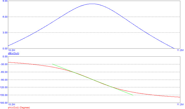
The only other design decision is what channel bandwidth and deviation are to be used. For an 'off-the-shelf' wideband FM transmission, the occupied bandwidth is a smidge over 250 kHz and the deviation is 75 kHz, so this is what the circuit will be designed for. The way in which the IC demodulates the FM signal is to apply the incoming signal to a tuned-circuit via a relatively high impedance inductor. The overall frequency and phase reponse of the circuit is shown in the figure below with frequency response in blue, and phase response in red.

As can be seen, there is a rapid change of phase as the frequency sweeps past 10.7 MHz, and it is this change which the IC uses to demodulate the audio of the FM transmission. The more linear the phase response, the less distorted the recovered modulation is. Ideally the phase change should be a straight line (a straight green line has been drawn on the graph for comparison). For low distortion demodulation of an FM signal at 10.7 MHz, the phase change line should be as flat as possible between approximately 10.575 and 10.825 MHz.
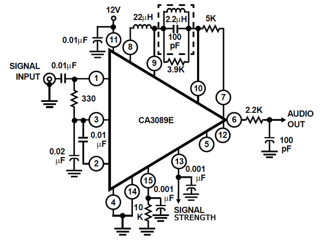
Changing the required bandwidth or deviation response of the receiver entails modifying these 'phase discriminator' components to alter their phase response. The circuit of a simple CA3089/3189 based FM demodulator is shown below. Note that there are a couple of small component differences between the CA3089 and CA3189 circuits.

Some of the pins are shown as being not connected. These relate to a 'mute' circuit which switches off the audio output of the device if there is no incoming signal (often called 'squelch'). This is very useful if being used for a hi-fi receiver as it means that when tuned to the emptiness between stations on the FM dial, the receiver goes quiet rather than emitting a loud hissing noise. It does, however, make it more difficult to eke out weak signals as if they are too weak, they will be muted and therefore they have been left unconnected.
add comment
( 300 views )
| permalink
| 


 ( 3 / 873 )


 ( 3 / 873 )
Monday 22 November, 2021, 20:32 - Amateur Radio, Broadcasting, Licensed, Pirate/Clandestine, Electronics
Posted by Administrator
Before addressing each of the building blocks required for a receiver, it is first important to consider the necessary gain distribution of the circuit and the various elements that make it up, that is to say the amount by which the signal needs to be amplified before it reaches the de-modulator. Set the gain too low and the receiver will lack sensitivity. Set the gain too high and not only is there a chance that it may self-oscillate due to the excessive gain, but the de-modulator may be driven with unnecessarily high signals which impede its performance.Posted by Administrator
The age old CA3089 (and the later CA3189) is still a good building block for a wide-band FM receiver as it has acceptably good noise performance, is easy to use, and has all the features needed (such as a signal strength indicator output) for most applications. The datasheet for the CA3089 shows that it begins to develop an audio output when the input to it reaches 12 microVolts. At this point it is 3dB down (half power) and rises to maximum output very quickly.
Now for some maths:
- Let us assume that the bandwidth of the receiver is 250 kHz (this is set by the IF filters) which is about correct for a wideband FM receiver.
- The amount of thermal (background) noise generated in 250 kHz of bandwidth into a 50 Ohm load is 0.45 microVolts - this is the amount of noise that would be naturally present at the input to the receiver based on the kTB formula where 'k' is Boltzmann's constant, T is the temperature of the receiver in degrees Kelvin (usually regarded as 290K) and B is the bandwidth in Hz.
- Note that man-made noise and other factors will increase this level at the antenna and thus the input level of the receiver will be somewhat higher. In addition, unless the receiver is noiseless (which is impossible) it will, itself, generate additional noise above and beyond this level, the amount of this is known as the noise figure or noise factor. However, let's use the thermal noise as the theoretical minimum input.
- The necessary voltage gain of the receiver from its RF input to the input of the CA3089 therefore needs to be a factor of 26.6 (12/0.45), or a power gain of 28 dB.
- The input band-pass filter may have a gain (actually a loss) of -2 dB (lower loss filters can be generated, but we shall be cautious in this regard).
- Mixers have not yet been discussed, however the NE602 which will be introduced later and used to perform the job of the mixer has a gain of +17 dB.
- This means that the IF stage which usually comprises a filter and an amplifier needs to have a gain of +13 dB to make the overall gain correct.
- A typical ceramic 10.7 MHz IF filter will have a loss of around -6 dB, meaning that to correct the overall gain, the IF amplifier needs approximately +19 dB of gain.

This arrangment of gain means that the de-modulator will see the background (thermal) noise as strong enough to begin to de-modulate audio. Any actual received signal will therefore be above this level and will be strong enough for the device to work correctly.
Thursday 4 November, 2021, 11:33 - Amateur Radio, Broadcasting, Licensed, Pirate/Clandestine, Electronics
Posted by Administrator
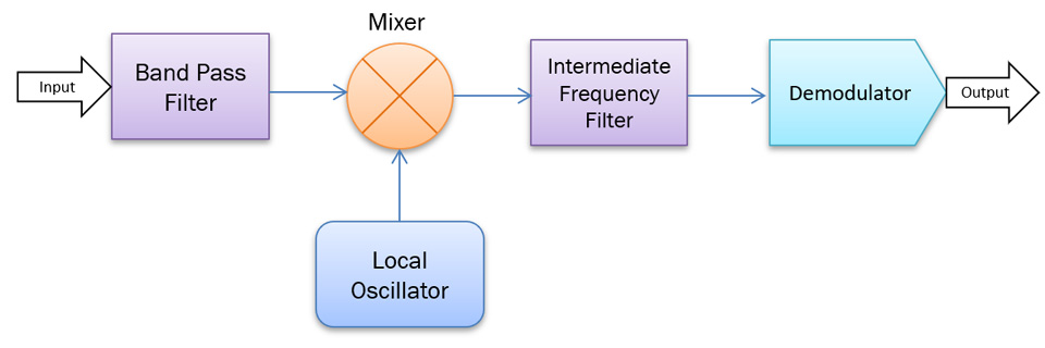
Now that the design of the transmitter has been completed, it's time to turn attention to a receiver. The diagram below shows the blocks which make up a receiver.Posted by Administrator

This works as follows:
- The incoming signal is first sent through a band-pass filter. The job of this filter is to ensure that only signals on the frequency (or frequencies) of interest are sent to the receiver. This makes the job of the receiver more straightforward and, in particular, needs to ensure that signals on the receiver's 'image' frequency (more of which later) are stopped from entering the next stages.
- Jumping to the end of the receiver, a second filter, the intermediate frequency (IF) filter has the job of filtering out any signals on frequencies adjacent to the one that is to be received. This filter has a much narrower frequency response than the band-pass filter at the receiver's input. For a wide-band FM signal, this would typcally have a bandwidth of 250 kHz, whereas the band-pass filter may cover 10 MHz or more.
- The de-modulator has the job of turning the received signal into some form of output. In the case of an FM receiver, this is audio, but this could equally be a digital output if the transmission was in some digital format.
- Sitting between the band-pass filter and the IF filter is a mixer, which is fed both the incoming received signal and some other frequency, usually generated by either a crystal (for a fixed frequency receiver) or by a PLL. This oscillator generating this signal is known as the local oscillator (LO). The mixer operates on the 'heterodyne' principal (invented in 1901 by Reginald Fessenden which is a story worthy of a future post). This mixer is non-linear and as such will 'mush up' the signals and produce all manner of other signals. If the incoming signals are two frequencies f1 and f2, then amongst other things, the mixer will produce 2xf1, 2xf2, f1-f2 (or vice versa), f1+f2 and many other variants. Of most interest to us are f1+f2 and f1-f2. If we take either of these outputs to be the frequency at the centre of the IF filter (usually 10.7 MHz), and f1 is the incoming signal, then if we set f2 at 10.7 MHz above or below the incoming signal frequency, one of the outputs from the mixer will be the IF frequency.
- Assume that the wanted receive frequency is 100 MHz and that the IF frequency is 10.7 MHz, then the LO needs to be at either 89.3 MHz (100-10.7) or 110.7 MHz (100+10.7).
- However, if the LO is at 89.3 MHz, the receiver will perform equally well, not just at 100 MHz but at 10.7 MHz below 89.3, i.e. 78.6 MHz (89.3-10.7). It is the job of the band-pass filter, therefore, to ensure that any signals at 78.6 MHz are rejected and that only the 100 MHz signal passes to the mixer.
- A similar situation occurs if the LO is at 110.7 MHz, as the receiver will then also receive signals at 121.4 MHz (110.7+10.7).
Choosing the correct LO frequency is not trivial and it is important to consider the image frequency. Take a receiver tuned to 71.6 MHz. This would have two possible image frequencies, depending on whether the LO is 10.7 MHz below or above 71.6 MHz. If the LO is below (i.e. 60.9 MHz) then the image frequency would be 50.2 MHz. If the LO is above (i.e. 82.3 MHz) then the image frequency would be 93 MHz. In the first instance the image frequency is right on top of the most active part of the amateur radio 6 metre band, and in the second it is on an FM band frequency. Either of these may lead to interference, and a well designed band-pass filter would be needed to ensure that only the wanted frequency was passed through.
One other important consideration is that receivers are, by their nature, very sensitive devices. Incoming signals as low as 1 microVolt are sufficient to produce an output. This means that very careful attention needs to be paid to the design, to ensure that the minimum of additional noise or unwanted signals are produced. This is especially the case if a PLL is used as the LO. The PLL needs to be clean. As discussed previously, pre-scalers used in PLL's can be very noisy, and care needs to be paid to ensure that none of the output from the pre-scaler is in any way capable of getting into the receiver. In addition, and digital signals (such as the output from the pre-scaler) need to be routed on tracks as short as possible, as, being square waves, they are full of harmonics which could easily fall on a frequency which would interfere with the receiver.
Lots to think about then, and in ensuing installments of this series, the additional building blocks needed for a receiver will be considered.
Monday 25 October, 2021, 19:46 - Amateur Radio, Broadcasting, Licensed, Pirate/Clandestine, Electronics
Posted by Administrator
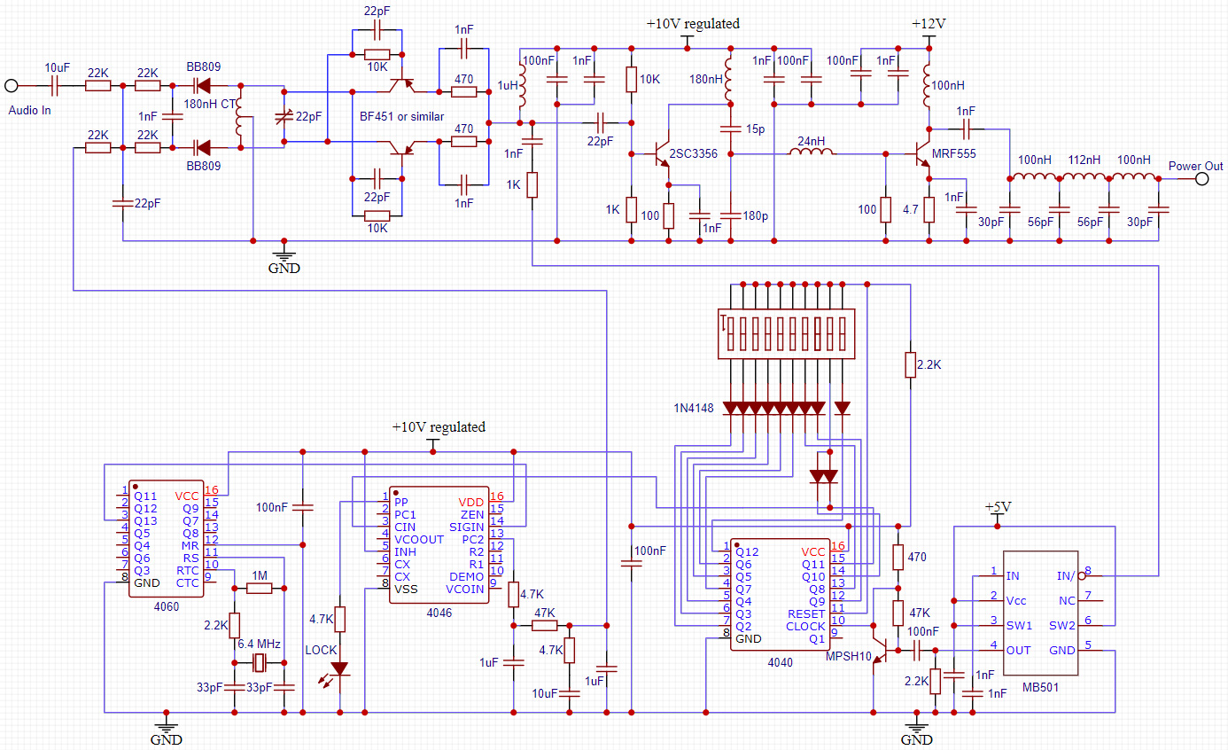
And so here it is, the completed 1 Watt phase locked loop (PLL) FM transmitter. The transmitter part is as exactly as described in part 12, so in this installment of 'How not to design transmitters and receivers' we shall examine the full transmitter including the phase locked loop (PLL). Posted by Administrator

Here's how it works... Some of the signal from the voltage controlled oscillator (VCO) has been tapped off via a 1 K resistor to reduce the amount that is fed to the pre-scaler. The oscillator provides more than sufficient output to feed both the pre-scaler and the transmitter, so there is no need in this case for any additional buffer between the VCO and the pre-scaler. The pre-scaler (the MB501L) is set to divide by 64 meaning, for example, that with the VCO operating at 100 MHz, the output will be at 1.5625 MHz. A single transistor NPN level buffer has been used between the pre-scalar and the 'divide by N' chip to increase the voltage from the approximately 1.5V peak-to-peak signal at the output of the MB501L to the full supply range needed for the CMOS chip.
Next the reference oscillator. A 4060 IC has been used, with a 6.4 MHz crystal. The division ratio of the 4060 that has been selected is 214 (oddly labelled Q13 in the schematic), or 16384, yielding an output from this chip at 390.625 Hz.
In order for the loop to lock, it is therefore necessary to divide the 1.5625 MHz coming from the pre-scaler down to 390.625 Hz. At an operating frequency of 100 MHz, this requires a division ratio of exactly 4000. If we wish the transmitter to operate over the whole of the FM band, for example, then we will require division ratios ranging from 3500 (for 87.5 MHz) to 4320 (for 108 MHz). The binary values for these ratios are shown in the table below.
| Digits | 212 | 211 | 210 | 29 | 28 | 27 | 26 | 25 | 24 | 23 | 22 | 21 | 20 |
|---|---|---|---|---|---|---|---|---|---|---|---|---|---|
| 4096 | 2048 | 1024 | 512 | 256 | 128 | 64 | 32 | 16 | 8 | 4 | 2 | 1 | |
| 3500 (87.5) | 0 | 1 | 1 | 0 | 1 | 1 | 0 | 1 | 0 | 1 | 1 | 0 | 0 |
| 4000 (100.0) | 0 | 1 | 1 | 1 | 1 | 1 | 0 | 1 | 0 | 0 | 0 | 0 | 0 |
| 4320 (108.0) | 1 | 0 | 0 | 0 | 0 | 1 | 1 | 1 | 0 | 0 | 0 | 0 | 0 |
A couple of things have been highlighted:
- Bits 10 and 11 (1024 and 2048) are either both '1' or both '0'. This holds true across the whole of the frequency range from 87.5 to 108.0 (indeed it holds true from binary 3072 [76.8] MHz to 5119 [127.975 MHz]). These two bits (coloured orange) can therefore be linked together.
- Bits 0 and 1 (1 and 2) are both '0' in both cases. This holds true for any frequency which is a mulitple of 100 kHz. These two bits can therefore be ignored.
A feed from Q11 has been taken from the chip to feed into the phase comparator. The phase comparator used is the good old (literally) 4046. This has two outputs of interest:
- The 'Pulse Phases' (PP) output (pin 1) goes low every time the phase comparator outputs an error voltage, meaning that if the loop is in lock, this pin sits at a positive voltage. Connecting an LED from this pin to ground (through a suitable current limiting resistor) thus acts as a lock detector, the LED growing increasingly bright as the PLL is locked. It can be informative to connect a headphone to this pin (via, say, a 4.7K resistor) as you will get an auditory indication of the two input frequencies and how far apart they are.
- The 'Phase Comparator 2' (PC2) output (pin 13) is used as the output of the phase detector itself. This pin will output a logic 'high' pulse if the divided down phase/frequency of the loop is lower than the reference frequency and a logic 'low' if the phase/frequency is too high. Suitably filtered, this output can be fed to the varicap diodes in the loop to correct the loop frequency.
No circuit for producing the necessary regulated 10 Volt (or 5 Volt) supply has been shown: If you can't work out how to produce such a voltage, there's little chance of you being able to build the transmitter correctly.
You have probably noted that this series is entitled 'How not to design transmitters and receivers', and so far all that has been covered are transmitters. So, in ensuing instalments, the building blocks required to build a receiver together with the many pitfalls which can trap you when doing this will be discussed.

