
How not to design transmitters and receivers: part 18 (IF amplifier)
Friday 24 June, 2022, 07:37 - Broadcasting, Licensed, Pirate/Clandestine, Electronics
Posted by Administrator
Next in the series of 'How not to design transmitters and receivers' we shall tackle the intermediate (IF) amplifier. This seemingly innocent little circuit is teeming with complexity and getting it right is not straightforward.Posted by Administrator
According to the calculations made in Part 15 of this series, the IF amplifier requires a gain of 19 dB or thereabouts (a few dB or so either way will not make too much difference). In addition, it needs to have an input and output impedance of 330 Ohms. This means that any ceramic filter used in the IF could be placed either before, or after, the amplifier and be correctly matched (or indeed two filters could be used). It is the combination of achieving a 330 Ohm input and output impedance, together with the requisite gain that makes the circuit more complex.
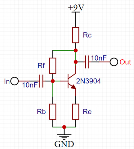
We shall use the circuit above as the basis for our amplifier. This is an untuned amplifier and will therefore provide gain across a wide range of frequencies which can sometimes cause problems as it will amplify both wanted and unwanted signals, however this has the major advantage that no tuning is required.
The gain of the circuit is primarily set by the ratio of Rc and Re, with gain being calculated as Rc divided by Re. However it needs to be remembered that Rc is in parallel with the load connected to the output, and that the transistor has an internal resistance in series with Re whose value is determined by the current flowing through the transistor (usually defined as 26 divided by the transistor emitter current (Ie in milliAmps).
Taking all this into account, the gain of the circuit can be (roughly) calculated by the equation:
Rc*Rload
(Rc+Rload)*(Re+26/Ie)
The input impedance of the circuit comprises three different values in parallel:
- Rb which is directly across the input of the circuit;
- The impedance of the emitter resistor Re (including the transistor's internal resistance) multiplied by the gain of the transistor (the Beta or hfe); and
- The impedance of the feedback resistor Rf divided by the gain of the transistor circuit (not the gain of the transitor itself).
1
1/Rb+1/(hfe*(Re+26/Ie))+1/(Rf/gaincircuit)
Rc*(Vcc-Rc*Ie)
Vcc
One final consideration is the transistor bias. Ideally, the output of the transistor would be set to have a voltage roughly half of that of the supply (give or take). This ensures that the output of the amplifier can swing up and down as far as possible before 'hitting the rails' and no longer amplifying. The output voltage (at the transistor's collector) is determined by Rc and the current passing through the transistor. The current passing through the transistor is determined by the current flowing into the base of the transistor multiplied by its gain. In the case where the bias current is set through the feedback resistor from the collector (Rf), this calculation is iterative, as the base current is then related to the collector current.
Another kink is that the collector current can also impact the gain of the transistor, with very low collector currents reducing the gain. Similarly, currents too high can have similar effects. It is necessary to consult the datasheet for the transistor being used to determine how the current affects the gain. Usually over a relatively wide range, the gain will be roughly constant (and be at its highest) and this is often the point that should be aimed for.
Hopefully, by now, you can see why getting the various resistor values correct is complicated, and how changing one value (such as the emitter resistor, or feedback resistor) can change the gain and impedances of the circuit.
The following values therefore produce an amplifier which meets, so far as is possible, all the criteria which are required for the IF gain stage:
- Rb = 2.2K Ohms
- Rc = 560 Ohms
- Re = 8.2 Ohms
- Rf = 10K Ohms
- The voltage gain of the amplifier is 17.8 (or 25 dB) before the reduction in gain caused by the feedback resistor Rf is taken into account;
- The input impedance of the amplifier is 331 Ohms;
- The output impedance of the amplifier is 299 Ohms.
Another set of values which yields the correct input and output impedances is:
- Rb = 1K Ohms
- Rc = 470 Ohms
- Re = 22 Ohms
- Rf = 4.7K Ohms
Note that in reality there are various additional factors which will impact the performance of the circuit, especially at radio frequencies. In particular, various capacitances within the transistor will tend to limit the high frequency performance. Choosing a transistor whose transition frequency (ft - the frequency at which the transistor's gain drops to unity) is significantly above the required amplifier frequency minimises these issues. According to its datasheet, the 2N3904 used in the amplifier has an (ft) of 300 MHz, and as we want the amplifier to operate at 10.7 MHz, this is sufficient margin to largely ignore these other factors.
add comment
( 3348 views )
| permalink
| 
 ( 3.1 / 1248 )
( 3.1 / 1248 )
How not to design transmitters and receivers: part 17 (PCB and kit)
Monday 7 March, 2022, 09:49 - Broadcasting, Licensed, Pirate/Clandestine, Electronics
Posted by Administrator
There seems to have been a lot of interest in the Wireless Waffle series entitled 'How Not to Design Transmitters and Receivers'. One or two (or, indeed, a few more) people have asked about a printed circuit board (PCB) layout and even whether it might be possible to put a kit of parts and set of instructions together for experimenters who wanted to try and build a 1 Watt FM transmitter/exciter for themselves. In that vein, a PCB has been designed for a simple synthesised PLL transmitter which has the following characteristics. It:
Posted by Administrator
- Uses a half-frequency oscillator, to get round the feedback problems that an at-frequency oscillator can suffer from in RF hot environments
- Is built from the minimum sub-set of components, to keep the cost of getting all the parts together as low as possible
- Doesn't use lots of obsolete, expensive or difficult-to-get-hold-of parts
- Can accommodate different output transistors (such as the 2N4427, MRF237 and similar)
- Can use a range of transistors for most of the parts (such as the BF199, MPSH10 and similar)
- Will produce around 1 Watt across the band with as little fiddling as possible (or more depending on the output transistor)
- Has an output that is legally clean enough to either be connected directly to an antenna, or amplified to high power (nothing over 60dB below the carrier)
- Keeps the digital and analogue parts of the circuit as seperate as possible to minimise digital noise on the modulation
- Doesn't require any micro-controllers and thus does not require any software to be written/blown
- Has out-of-lock power-down to stop transmissions on unwanted frequencies whilst the phase lock loop is settling down
- Is straightforward to set onto the desired frequency
- Can be easily tested and maintained (to the extent that it could be built in stages, testing each along the way)
- Has a flat modulation frequency response from around 3 Hz to at least 100 kHz, providing superlative audio
- Does not need any tuning (other than setting the VCO frequency)
- Can have its output quickly disabled (i.e. for connection to a high SWR detector)
- With some component changes, can be made to work on Band-I too (the final design will work down to about 52 MHz)
There are no surface-mount parts on the PCBs, making it easy to assemble even for the relatively cack-handed, and the ICs can be socketted for those not confident enough to solder the chips directly to the board. The only complexity is that there are a number of coils to be manually wound, including one on a small toroid.
The circuit diagram is below and those who have followed the series will recognise the various elements which go together to make up the overall design.
;)
Three options are available for anyone who wishes to have a go a building this design:
- PBC's for this project are available on their own for those who wish to assemble the various components required themselves, or who have a large junk-box full of suitable components. This is £4.99 plus postage.
- In addition, a minimalist kit is available which contains the PCB, as well as the ICs, transistors and the toroid and wire for winding the coils as these are the parts least likely to be in a typical junk box. This is £24.99 plus postage.
- Finally, a full kit of parts is available including the PCB, semi-conductors, toroids and all the resistors, capacitors and diodes needed to complete the project. This is £34.99 plus postage.
To get hold of your FM 3.05K kit, please leave a postcard with your name and address, together with £10,000 in unmarked £20 notes in a rucksack in a dustbin of your choice at Piccadilly railway station in Manchester at 23:15 any sunny Tuesday night in March.
Alternatively, fill in the contact form, stating which version of the kit you wish to purchase, and where it needs posting to, and we'll get back to you with a final price (including the postage) and how to pay (this will be via PayPal).

How not to design transmitters and receivers: part 16 (FM demodulator)
Thursday 9 December, 2021, 15:57 - Amateur Radio, Broadcasting, Licensed, Pirate/Clandestine, Electronics
Posted by Administrator
In the grand tradition of Wireless Waffle, instead of starting at the beginning of the receiver design, we shall tackle the end, the de-modulator, first. There are a number of ICs that will de-modulate wideband FM signals including modern chips which can act as a complete receiver chain. Notwithstanding these, however, the age old (actually 40 year old) CA3089 and CA3189 (a.k.a. HA1137) are capable IC's which have both technical and economic advantages:
Posted by Administrator
- They are easy to work with, requiring few external parts.
- They can be modified to work with different channel bandwidths and deviations.
- They yield very decent audio signal to noise ratios for strong signals (in excess of 70 dB).
- They have decent AM rejection (i.e. the ability to ignore signal fluctuations).
- They have relatively low audio distortion (around 0.5% THD in a standard configuration).
- They are easy to get hold of.
- They are cheap.
Intermediate frequency (IF) filters typically used in wideband FM receivers are usually based on ceramic filters which almost always have an impedance around 330 Ohms. This means that the input impedance of the de-modulator must be 330 Ohms to match the filter properly and ensure that the performance and frequency response of the filter are correctly achieved. The input impedance of the CA3089/3189 itself is not specified in the datasheet but is generally regarded as being 'high' (i.e. a few kilo Ohms). As such, to match the 330 Ohm impedance of the filter it is simply a matter of placing a 330 Ohm resistor across the input of the chip, as the effect of the parallel input impedance of the chip would be negilgable.
The only other design decision is what channel bandwidth and deviation are to be used. For an 'off-the-shelf' wideband FM transmission, the occupied bandwidth is a smidge over 250 kHz and the deviation is 75 kHz, so this is what the circuit will be designed for. The way in which the IC demodulates the FM signal is to apply the incoming signal to a tuned-circuit via a relatively high impedance inductor. The overall frequency and phase reponse of the circuit is shown in the figure below with frequency response in blue, and phase response in red.
;)
As can be seen, there is a rapid change of phase as the frequency sweeps past 10.7 MHz, and it is this change which the IC uses to demodulate the audio of the FM transmission. The more linear the phase response, the less distorted the recovered modulation is. Ideally the phase change should be a straight line (a straight green line has been drawn on the graph for comparison). For low distortion demodulation of an FM signal at 10.7 MHz, the phase change line should be as flat as possible between approximately 10.575 and 10.825 MHz.
Changing the required bandwidth or deviation response of the receiver entails modifying these 'phase discriminator' components to alter their phase response. The circuit of a simple CA3089/3189 based FM demodulator is shown below. Note that there are a couple of small component differences between the CA3089 and CA3189 circuits.
;)
Some of the pins are shown as being not connected. These relate to a 'mute' circuit which switches off the audio output of the device if there is no incoming signal (often called 'squelch'). This is very useful if being used for a hi-fi receiver as it means that when tuned to the emptiness between stations on the FM dial, the receiver goes quiet rather than emitting a loud hissing noise. It does, however, make it more difficult to eke out weak signals as if they are too weak, they will be muted and therefore they have been left unconnected.
How not to design transmitters and receivers: part 15 (receiver gain distribution)
Monday 22 November, 2021, 20:32 - Amateur Radio, Broadcasting, Licensed, Pirate/Clandestine, Electronics
Posted by Administrator
Before addressing each of the building blocks required for a receiver, it is first important to consider the necessary gain distribution of the circuit and the various elements that make it up, that is to say the amount by which the signal needs to be amplified before it reaches the de-modulator. Set the gain too low and the receiver will lack sensitivity. Set the gain too high and not only is there a chance that it may self-oscillate due to the excessive gain, but the de-modulator may be driven with unnecessarily high signals which impede its performance.Posted by Administrator
The age old CA3089 (and the later CA3189) is still a good building block for a wide-band FM receiver as it has acceptably good noise performance, is easy to use, and has all the features needed (such as a signal strength indicator output) for most applications. The datasheet for the CA3089 shows that it begins to develop an audio output when the input to it reaches 12 microVolts. At this point it is 3dB down (half power) and rises to maximum output very quickly.
Now for some maths:
- Let us assume that the bandwidth of the receiver is 250 kHz (this is set by the IF filters) which is about correct for a wideband FM receiver.
- The amount of thermal (background) noise generated in 250 kHz of bandwidth into a 50 Ohm load is 0.45 microVolts - this is the amount of noise that would be naturally present at the input to the receiver based on the kTB formula where 'k' is Boltzmann's constant, T is the temperature of the receiver in degrees Kelvin (usually regarded as 290K) and B is the bandwidth in Hz.
- Note that man-made noise and other factors will increase this level at the antenna and thus the input level of the receiver will be somewhat higher. In addition, unless the receiver is noiseless (which is impossible) it will, itself, generate additional noise above and beyond this level, the amount of this is known as the noise figure or noise factor. However, let's use the thermal noise as the theoretical minimum input.
- The necessary voltage gain of the receiver from its RF input to the input of the CA3089 therefore needs to be a factor of 26.6 (12/0.45), or a power gain of 28 dB.
- The input band-pass filter may have a gain (actually a loss) of -2 dB (lower loss filters can be generated, but we shall be cautious in this regard).
- Mixers have not yet been discussed, however the NE602 which will be introduced later and used to perform the job of the mixer has a gain of +17 dB.
- This means that the IF stage which usually comprises a filter and an amplifier needs to have a gain of +13 dB to make the overall gain correct.
- A typical ceramic 10.7 MHz IF filter will have a loss of around -6 dB, meaning that to correct the overall gain, the IF amplifier needs approximately +19 dB of gain.
;)
This arrangment of gain means that the de-modulator will see the background (thermal) noise as strong enough to begin to de-modulate audio. Any actual received signal will therefore be above this level and will be strong enough for the device to work correctly.