
Bilsdale versus Eston Nab
Around a million people in the North East of England in areas from Sunderland to Whitby, including Hartlepool, Darlington and Middlesborough came home from work on 10 August to find that their Freeview TV, DAB radio and FM radio services had disappeared. This was caused by a fire at the Bilsdale mast in the North Yorkshire moors. At the time of writing, it is still unclear whether the masts's structure is sound and as an interim, transmission company Arqiva are putting a number of mitigations in place to try and restore services.
One of the main mitigations which has already been put in place is to move the DTT services from Bilsdale to a mast at Eston Nab. Eston Nab was previously a relay station used to provide fill-in TV coverage to a few homes around Eston, Teesville and Wilton who, ironically, could not receive a service from Bilsdale as the Nab itself blocked the line-of-sight. The relay station originally had a transmitter power of just 3 Watts (compare this to the 100,000 Watts which Bilsdale used)
Eston Nab was also used as a high power FM transmitter for Smooth Radio on 107.7 with a power of 2.5 kW. Most of the rest of the FM stations in the region were transmitted from the Bilsdale mast at a power of 5 kW. Though TV services which previously ran at Bilsdale have been relocated to Eston Nab, the transmitter power in use is far lower. One report claims that the power of the new DTT TV transmitters at Eston Nab are just 20 Watts.
Wireless Waffle wondered how the coverage from Eston Nab would compare to Bilsdale if it ended up being needed in the long term due to the Bilsdale mast needing to be re-built completely. Though it is not a direct like-for-like comparison, the Associated Broadcasting Consultants web-site provides coverage maps for FM radio services based on the parameters provided by Ofcom. As such, it is possible to compare the coverage of the Smooth Radio 107.7 FM service from Eston Nab with, for example, the previous coverage of the Heart FM 100.7 FM service from Bilsdale.
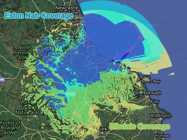
The map above compares the coverage of the Smooth and Heart FM services from the two transmitter sites. Coverage from Bilsdale is in green and yellow, and coverage from Eston Nab is in blue and aqua. When it comes to the larger cities in the region (Darlington, Middlesborough and Hartlepool) it is clear that it may be possible to restore service from the Eston Nab transmitter as this provides reasonable coverage in these areas. Across the North Yorkshire Moors however, the Eston Nab transmitter does not provide much by the way of coverage. For these locations, an alternative may be necessary.
Note that the map compares coverage for FM transmitters and at the UHF frequencies used by television, coverage would be far more patchy, however it does suggest that a higher power site at Eston Nab may restore coverage in some of the more densely populated affected areas. Note that in these areas, the direction of the Eston Nab transmitter would be different to Bilsdale which would require the re-pointing of TV antennas for many people (this is not an issue for FM reception as most antennas, such as those on cars, are not directional).
An additional plan being considered is to use the BT microwave tower at Arncliffe Wood to restore service in and around Northallerton, Thirsk and Malton. Again, re-pointing of antennas may be necessary in these areas. It is possible that further sites may be identified which, working together, could restore coverage to the original Bilsdale coverage area without the need to re-build the mast (should this prove necessary). Such schemes have been used before. In Portugal, for example, the national DTT service is provided from a network of cellphone towers, rather than the large hill-top sites previously used for the analogue service.
Useful links:
One of the main mitigations which has already been put in place is to move the DTT services from Bilsdale to a mast at Eston Nab. Eston Nab was previously a relay station used to provide fill-in TV coverage to a few homes around Eston, Teesville and Wilton who, ironically, could not receive a service from Bilsdale as the Nab itself blocked the line-of-sight. The relay station originally had a transmitter power of just 3 Watts (compare this to the 100,000 Watts which Bilsdale used)
Eston Nab was also used as a high power FM transmitter for Smooth Radio on 107.7 with a power of 2.5 kW. Most of the rest of the FM stations in the region were transmitted from the Bilsdale mast at a power of 5 kW. Though TV services which previously ran at Bilsdale have been relocated to Eston Nab, the transmitter power in use is far lower. One report claims that the power of the new DTT TV transmitters at Eston Nab are just 20 Watts.
Wireless Waffle wondered how the coverage from Eston Nab would compare to Bilsdale if it ended up being needed in the long term due to the Bilsdale mast needing to be re-built completely. Though it is not a direct like-for-like comparison, the Associated Broadcasting Consultants web-site provides coverage maps for FM radio services based on the parameters provided by Ofcom. As such, it is possible to compare the coverage of the Smooth Radio 107.7 FM service from Eston Nab with, for example, the previous coverage of the Heart FM 100.7 FM service from Bilsdale.
;)
The map above compares the coverage of the Smooth and Heart FM services from the two transmitter sites. Coverage from Bilsdale is in green and yellow, and coverage from Eston Nab is in blue and aqua. When it comes to the larger cities in the region (Darlington, Middlesborough and Hartlepool) it is clear that it may be possible to restore service from the Eston Nab transmitter as this provides reasonable coverage in these areas. Across the North Yorkshire Moors however, the Eston Nab transmitter does not provide much by the way of coverage. For these locations, an alternative may be necessary.
Note that the map compares coverage for FM transmitters and at the UHF frequencies used by television, coverage would be far more patchy, however it does suggest that a higher power site at Eston Nab may restore coverage in some of the more densely populated affected areas. Note that in these areas, the direction of the Eston Nab transmitter would be different to Bilsdale which would require the re-pointing of TV antennas for many people (this is not an issue for FM reception as most antennas, such as those on cars, are not directional).
An additional plan being considered is to use the BT microwave tower at Arncliffe Wood to restore service in and around Northallerton, Thirsk and Malton. Again, re-pointing of antennas may be necessary in these areas. It is possible that further sites may be identified which, working together, could restore coverage to the original Bilsdale coverage area without the need to re-build the mast (should this prove necessary). Such schemes have been used before. In Portugal, for example, the national DTT service is provided from a network of cellphone towers, rather than the large hill-top sites previously used for the analogue service.
Useful links:
- Arqiva update on the Bilsdale mast incident
- Measured coverage area maps
- MB21 updates on plans to restore service
- UKfreeTV page on the Bilsdale transmitter
- Twitter feed of a516digital providing additional information on the situation
add comment
( 152 views )
| permalink
| 

 ( 2.5 / 357 )
( 2.5 / 357 )
Tropospheric vs Sporadic-E Propagation Loss
Wednesday 18 August, 2021, 09:35 - Broadcasting, Licensed, Radio Randomness, Spectrum Management
Posted by Administrator
For some time, Wireless Waffle has published an FM DX Logbook. This logbook records any DX (distance) reception of FM broadcast stations that have been received, through whatever means (i.e. home FM tuner, car radio, software radio). Though an interesting exercise in itself, a recent update to the page to show the propagation mode which has been used also included some simple calculations to show the number of metres travelled divided by the number of Watts of transmitter power, and an additional calculation working out what the received signal power would be, assuming free space path loss between the transmitting and receiving location.Posted by Administrator
The use of free space path loss as the propagation model is definitely not applicable for any mode of propagation other than line-of-sight but it proved to be a useful exercise. Based on the frequency and power of the transmitter, and the length of the path, it is possible to determine how strong the received signal would be, if the path was line-of-sight. The results show an interesting trend.
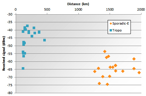
With the exception of a few shorter paths (up to about 150 km), the theoretical signal strengths received from broadcasts received via troposhperic propagation are clustered around -40 dBm (which equates to about 67 dBuV/m). Similarly, the theoretical signal strength of transmissions received via Sporadic-E propagation are clustered around -65 dBm (42 dBuV/m). Note that these are not measured signal strengths, but a calculation of how strong the signals would be if they were being received via a line-of-sight path - which they are not.
A previous Wireless Waffle article identified that around 40dBuV/m is required at a receiver for FM reception. It is almost certainly true, that in the case of both the DX reception via the troposphere, or via Sporadic-E, the actual received signal strength would be similar, as in both cases the signal would need to be strong enough to be successfully received: the necessary signal would be nearer the -65 dBm level than the -40 dBm level. If this is true, then it must also be true that the additional loss caused by a signal travelling via ducts in the troposphere compared to via ionised clouds in the E-layer is around 25 dB, as this is the additional loss which the signal could tolerate and still be received.
This just goes to show how effective Sporadic-E propagation is and why it is (or indeed was) such a problem for VHF television and radio broadcasters during the summer months when it is most prevalent. It also suggests that the path loss via Sporadic-E must be close to the free space value, as if the received signal strength is around 42 dBuV/m based on free space path loss, this is only a couple of dB different to that needed for successful reception and the actual path could not be introducing much in the way of additional attenuation.
How not to design transmitters and receivers (part 5: phase locked loops)
Thursday 12 August, 2021, 09:39 - Amateur Radio, Broadcasting, Licensed, Pirate/Clandestine, Electronics, Radio Randomness
Posted by Administrator
Parts 1 to 4 of this series have covered generating an RF signal, amplifying it, and providing the whole kit and caboodle with a nice clean power supply. In this part, we consider frequency stabilisation.Posted by Administrator
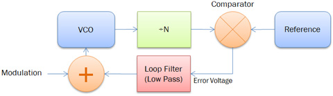
It is very straightfoward to produce a radio frequency (RF) signal that does not drift from the wanted frequency. Using a quartz crystal oscillator, it is possible to maintain an accuracy of a few parts per million, or a couple of Hz per MHz of output frequency. However, the output from a crystal is so stable that it's just about impossible to move it. If you want to modulate the frequency by more than a few kHz, using a crystal is therefore not feasible. For a wideband FM transmitter, where the required deviation (i.e. the amount by which the frequency changes) is +/- 75 kHz, using a crystal is therefore a non-starter. Instead it is necessary to use a voltage controlled oscillator (VCO) and surround this by some kind of feedback loop which samples the output frequency and corrects it if it has drifted off the wanted frequency. Such a feedback loop is called a phase locked loop or PLL (or indeed a frequency locked loop).
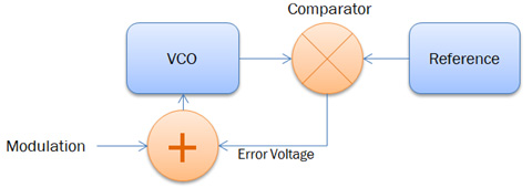
A simple PLL would just compare the frequency being produced by an VCO with some reference, determine the difference between the two, and if the two are different, provide an error voltage to the VCO to bring it back onto frequency. In the block diagram above, the error voltage is added to the modulation voltage as both of them affect the frequency of oscillation. This system would be great, and work a treat, if it was only necessary to operate on one frequency. However, if it is necessary to tune the VCO to different frequencies, some additional jiggery pokery is necessary.
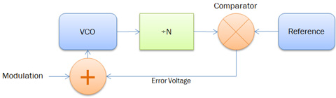
To make a tuneable PLL, an additional stage is added to the loop. The output from the VCO is divided by a number (let's call it 'N') and instead of having a reference frequency the same as the wanted output frequency, a much lower reference frequency is used. For example, if the reference frequency is 100 kHz, and we wanted the VCO to be on 89.6 MHz, we would divide the VCO output by 896 to give 100 kHz, and compare this to the 100 kHz reference. The rest of the circuit then operates as before. If we now change the division ratio to 900 instead of 896, the circuit would now attempt to retune the output to 90.0 MHz (assuming that the VCO was able to tune to that frequency). Thus, by changing the division ratio, we can lock the output frequency to any multiple of the reference frequency that we desire.
One difficulty of using a PLL in the case where we are trying to modulate the VCO (for example with audio or data) is that the PLL will see any modulation as a frequency error and try and correct it. To circumvent this problem it is normal to filter the error voltage produced by the PLL such that it cannot act upon the VCO at any frequency we are interested in modulating. If we are interested in audio frequencies which may descend as low as 20 Hz, we therefore need to low pass filter the error signal so that it cannot have any effect on modulation frequencies above 20 Hz and thus cannot try and 'correct' the audio being modulated onto the VCO.
This low pass filter is known as the loop filter. In addition to ensuring that the response of the loop is slow enough not to impact any low frequency modulation, it has the dual purpose of removing any of the reference frequency that might be present on the error voltage as the output of the comparator output will often just be a square wave whose mark-space ratio changes depending on the difference between the VCO frequency and the reference. If the required loop response time is slower than 20 Hz, and the reference frequency is 100 kHz this is not a difficult job, however having such a difference between the loop response time and the reference frequency leads to another difficulty: overshoot.
Imagine the situation...
- We switch on the PLL and the output frequency of the VCO is too low. The comparator recognises this and outputs a positive voltage to tell the VCO to increase its frequency. This positive signal is filtered by the loop filter which has the effect of slowing down the response time, and the VCO slowly begins to respond and its frequency rises.
- At some point the VCO output and the reference will now be the same and the comparator will stop producing a positive correction, however the loop filter, being very slow in comparison, has not yet finished acting upon its previous 'increase frequency' instruction and so instead of the PLL settling down, the output frequency continues to rise above the wanted one.
- The comparator now recognises that the frequency is too high and outputs a negative voltage to tell the VCO to reduce its output frequency. This instruction is slowed down by the laggard of the loop filter.
- Eventually the VCO output matches the reference and the comparator stops issuing its correction. But the loop filter has not yet finished the 'reduce frequency' instruction it was given and so the VCO frequency continues to go down.
- The comparator recognises this and outputs a positive voltage to tell the VCO to increase its frequency...
One solution to this is to speed up the loop filter response, but this would then mean that lower modulating frequencies would be corrected by the PLL. Another solution is to reduce the reference frequency so that the loop frequency and the reference frequency are sufficiently close that one does not lag the other too much. This, however, often means that the loop filter will not be able to filter out the comparator output sufficiently, leading to the reference frequency modulating the VCO and causing 'spurs' in the RF output that are separated from the VCO output by the reference frequency.
A common solution to the yo-yo problem is to use a 'lead-lag' filter instead of just a low-pass for the loop filter. A lead-lag filter is a low pass filter whose frequency response is flattened at some point in its frequency range. The advantage of this is that it can provide the filtering necessary to slow down the loop and get rid of the comparator output, whilst providing protection against the yo-yo-ing by having a flatter phase response. This can then be combined with a seperate filter to specifically remove the comparator output and together the two can ensure good performance and a clean VCO output.
How not to design transmitters and receivers (part 4: low drop-out regulators)
Tuesday 3 August, 2021, 07:50 - Amateur Radio, Broadcasting, Licensed, Pirate/Clandestine, Electronics
Posted by Administrator
A quick diversion from RF design to consider, for a short while, the issue of voltage regulation. Voltage Controlled Oscillators (VCOs) need to be supplied with a well regulated and low noise power supply. The power for most equipment is either provided via a mains power supply (which can be full of noise and buzz) or a battery (whose output voltage will decrease over time). Therefore, some manner of regulator is required in order to stabilise the supply and reduce any noise on the supply rail. There are several ways to achieve this:Posted by Administrator
- fixed discrete voltage regulators,
- variable discrete voltage regulators, or
- a purpose designed circuit.
The problem with getting a regulated 10 Volt supply from a 12 Volt input is that the amount of headroom available in which the regulator is able to operate is very limited (just 2 Volts in fact). 10 Volt fixed discrete regulators do exist. The 7810 is one such device, however the datasheet for these regulators clearly states:
The input voltage must remain typically 2.0V above the output voltage even during the low point on the input ripple voltage.
;) So whilst 12 Volts at the input would be just about sufficient to allow the device to do its job, if the input dropped to even 11.9 Volts, there is no guarantee that the regulated output would remain at 10 Volts. The situation is actually more complicated than that, and the necessary voltage drop across the device in order for it to be able to do its job depends on the amount of current it is supplying and the temperature of the device. At low currents and high temperatures the necessary differential between the input and output voltage (the 'dropout' voltage) can be as low as 0.75 Volts, whereas at high current and low temperatures it can reach over 2.2 Volts. Thus, though in principle such a device could provide the 10 Volt regulated supply required, it would be working at the edge of its tolerances and may not provide quite as much regulation as desired.
So whilst 12 Volts at the input would be just about sufficient to allow the device to do its job, if the input dropped to even 11.9 Volts, there is no guarantee that the regulated output would remain at 10 Volts. The situation is actually more complicated than that, and the necessary voltage drop across the device in order for it to be able to do its job depends on the amount of current it is supplying and the temperature of the device. At low currents and high temperatures the necessary differential between the input and output voltage (the 'dropout' voltage) can be as low as 0.75 Volts, whereas at high current and low temperatures it can reach over 2.2 Volts. Thus, though in principle such a device could provide the 10 Volt regulated supply required, it would be working at the edge of its tolerances and may not provide quite as much regulation as desired.Variable voltage discrete regulators (such as the LM317) work on a similar principle to fixed ones, however they are designed to provide a variable output voltage instead of a fixed one. They usually have a reference source of around 1.2 Volts against which another voltage is compared. For example, if you wanted a 12 Volt regulated output, you would use two resistors, one (for the sake of argument) of 900 Ohms, and one of 100 Ohms, connected in series across the output of the power supply. The voltage at the junction of these two resistors when the output voltage was exactly 12 Volts would be 1.2 Volts (12 x 100 / [900+100]). Feed this to the 'comparison' input on the device and it would compare this voltage to its internal 1.2 Volt reference and adjust its output to maintain equilibrium. Thus, by tweaking the value of the resistors, virtually any voltage can be generated. One issue with such a device is that its minimum dropout voltage is generally the same as that of a fixed regulator (as the internal architecture of the devices is much the same) and thus it is also working at the edge of its capabilities with a 2 Volt dropout.
It should be noted that there are a range of Low Dropout (LDO) regulators which can function with much smaller dropout voltages. For example the LM2931 which can operate with a dropout as little as 0.4 Volts. Whilst these may be ideal for this purpose, they aren't readily available in 10 Volt versions and they are not cheap (at least not compared with non-LDO equivalents).
Of course, the Wireless Waffle lockdown radio project could have just decided on using a 9 Volt regulated supply, or an LDO regulator both of which are relatively straightforward, instead of looking to achieve 10 Volts, but what would be the fun in that. Instead the third option of purpose designing a regulator was explored.
The 'bog standard' LDO regulator design which is presented on various forums on the internet is as shown in the circuit below.
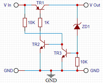
It works on the basis that as the output voltage increases to the point that the Zener diode conducts, the voltage at the base of NPN transistor TR3 increases and as it approaches 0.7 Volts it begins to turn-on. As it does this, it clamps the base voltage of the other NPN transistor, TR2, which turns-off and in the process reduces the current flowing into the base of the PNP transistor TR1 which also turns off reducing the current flowing through it, and thereby lowering the circuit's output voltage (and vice versa for a decrease in output voltage). The output voltage of the regulator is therefore set by the voltage of the Zener diode, ZD1, plus the turn-on voltage of transistor TR3. The reason that this is a low dropout regulator is that the dropout is determined only by the minimum collector-emitter voltage of the PNP transistor, TR1, when it is turned fully on, and this can be as low as 0.2 Volts. The primary issue with this circuit is that its ability to regulate the output voltage is based partially on the turn-on voltage at the base of TR3 and all bipolar transistors are very prone to changes in their turn-on voltage with temperature.
In addition, Zener diodes do not come in every possible Voltage (the nearest you could get to give a 10 Volt output would be to use a 9.1V Zener which together with the turn-on voltage of the transistor of about 0.7 Volts would yield a 9.8 Volt output). Zener diodes are also, like the junction in a bipolar transistor, prone to temperature drift. Thus, what might be a perfect 9.8 Volt output at room temperature might drop to 9.6 Volts at 50C or 10 Volts at -10C - not particularly well regulated.
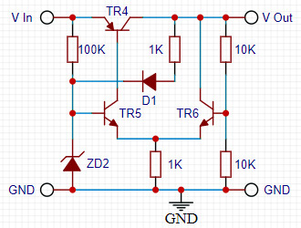
An alternative design (shown above) uses a 'long-tailed pair' (TR5 and TR6) and also uses a Zener diode to provide the voltage reference. Zener diodes of values around 6 Volts have virtually constant temperature characteristics meaning that if used as the voltage reference in a regulator, the output will vary very little as it heats up or cools down. Zener diodes typically need about 5mA of current passing through them to achieve a stable reference voltage and this can be provided from the regulated supply (through D1 and the 1K resistor), ensuring a near constant reference voltage.
The long-tailed pair basically function as an inverter: What one transistor does, the other does the opposite. So if the current in one transistor increases, the current in the other one decreases. The base of NPN transistor TR5 is provide with a fixed voltage reference by the Zener diode, whilst the base of the other senses the output voltage of the circuit via the potential divider made up of the two 10K resistors. The circuit will try and balance the voltage at both bases as follows: If the output voltage decreases, transistor TR6 will draw less current (as its base voltage decreases) and by dint transistor TR5 will draw more current, which forces more current into the base of the PNP transistor, TR4, which will conduct more heavily and increase the output voltage and behold the output voltage is stabilised.
As with a variable regulator, the output voltage can be adjusted by changing the value of the two 10K resistors. As it sits, the output voltage would be exactly 2 times the voltage across the Zener diode. The 100K resistor, by the way, is to provide some initial current for the Zener diode; otherwise, when the circuit is initialised, the Zener voltage and output voltage would both be zero and the circuit would be in equilibrium and nothing else would happen.
This may seem a silly length to go to to produce a low dropout regulator when off-the-shelf ones are available, but oddly, the design using discrete components takes up little more space on a circuit board, performs just as well, and is cheaper. It is also surprisingly good at getting rid of supply hum, buzz, ripple and noise. In addition, if the diode in the circuit (D1) is replaced by a light emitting one (an LED) it will provide an indication that all is well with the regulated output: your off-the-shelf regulator doesn't do that for you now does it?