Monday 25 October, 2021, 19:46 - Amateur Radio, Broadcasting, Licensed, Pirate/Clandestine, Electronics
Posted by Administrator
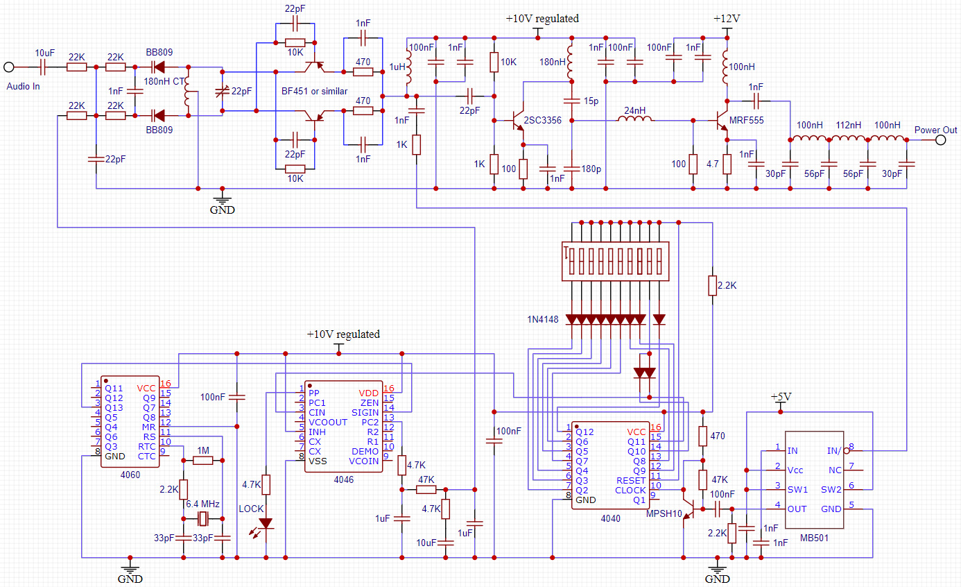
And so here it is, the completed 1 Watt phase locked loop (PLL) FM transmitter. The transmitter part is as exactly as described in part 12, so in this installment of 'How not to design transmitters and receivers' we shall examine the full transmitter including the phase locked loop (PLL). Posted by Administrator

Here's how it works... Some of the signal from the voltage controlled oscillator (VCO) has been tapped off via a 1 K resistor to reduce the amount that is fed to the pre-scaler. The oscillator provides more than sufficient output to feed both the pre-scaler and the transmitter, so there is no need in this case for any additional buffer between the VCO and the pre-scaler. The pre-scaler (the MB501L) is set to divide by 64 meaning, for example, that with the VCO operating at 100 MHz, the output will be at 1.5625 MHz. A single transistor NPN level buffer has been used between the pre-scalar and the 'divide by N' chip to increase the voltage from the approximately 1.5V peak-to-peak signal at the output of the MB501L to the full supply range needed for the CMOS chip.
Next the reference oscillator. A 4060 IC has been used, with a 6.4 MHz crystal. The division ratio of the 4060 that has been selected is 214 (oddly labelled Q13 in the schematic), or 16384, yielding an output from this chip at 390.625 Hz.
In order for the loop to lock, it is therefore necessary to divide the 1.5625 MHz coming from the pre-scaler down to 390.625 Hz. At an operating frequency of 100 MHz, this requires a division ratio of exactly 4000. If we wish the transmitter to operate over the whole of the FM band, for example, then we will require division ratios ranging from 3500 (for 87.5 MHz) to 4320 (for 108 MHz). The binary values for these ratios are shown in the table below.
| Digits | 212 | 211 | 210 | 29 | 28 | 27 | 26 | 25 | 24 | 23 | 22 | 21 | 20 |
|---|---|---|---|---|---|---|---|---|---|---|---|---|---|
| 4096 | 2048 | 1024 | 512 | 256 | 128 | 64 | 32 | 16 | 8 | 4 | 2 | 1 | |
| 3500 (87.5) | 0 | 1 | 1 | 0 | 1 | 1 | 0 | 1 | 0 | 1 | 1 | 0 | 0 |
| 4000 (100.0) | 0 | 1 | 1 | 1 | 1 | 1 | 0 | 1 | 0 | 0 | 0 | 0 | 0 |
| 4320 (108.0) | 1 | 0 | 0 | 0 | 0 | 1 | 1 | 1 | 0 | 0 | 0 | 0 | 0 |
A couple of things have been highlighted:
- Bits 10 and 11 (1024 and 2048) are either both '1' or both '0'. This holds true across the whole of the frequency range from 87.5 to 108.0 (indeed it holds true from binary 3072 [76.8] MHz to 5119 [127.975 MHz]). These two bits (coloured orange) can therefore be linked together.
- Bits 0 and 1 (1 and 2) are both '0' in both cases. This holds true for any frequency which is a mulitple of 100 kHz. These two bits can therefore be ignored.
A feed from Q11 has been taken from the chip to feed into the phase comparator. The phase comparator used is the good old (literally) 4046. This has two outputs of interest:
- The 'Pulse Phases' (PP) output (pin 1) goes low every time the phase comparator outputs an error voltage, meaning that if the loop is in lock, this pin sits at a positive voltage. Connecting an LED from this pin to ground (through a suitable current limiting resistor) thus acts as a lock detector, the LED growing increasingly bright as the PLL is locked. It can be informative to connect a headphone to this pin (via, say, a 4.7K resistor) as you will get an auditory indication of the two input frequencies and how far apart they are.
- The 'Phase Comparator 2' (PC2) output (pin 13) is used as the output of the phase detector itself. This pin will output a logic 'high' pulse if the divided down phase/frequency of the loop is lower than the reference frequency and a logic 'low' if the phase/frequency is too high. Suitably filtered, this output can be fed to the varicap diodes in the loop to correct the loop frequency.
No circuit for producing the necessary regulated 10 Volt (or 5 Volt) supply has been shown: If you can't work out how to produce such a voltage, there's little chance of you being able to build the transmitter correctly.
You have probably noted that this series is entitled 'How not to design transmitters and receivers', and so far all that has been covered are transmitters. So, in ensuing instalments, the building blocks required to build a receiver together with the many pitfalls which can trap you when doing this will be discussed.
add comment
( 352 views )
| permalink
| 


 ( 3 / 1339 )


 ( 3 / 1339 )

