
How not to design transmitters and receivers (part 5: phase locked loops)
Thursday 12 August, 2021, 09:39 - Amateur Radio, Broadcasting, Licensed, Pirate/Clandestine, Electronics, Radio Randomness
Posted by Administrator
Parts 1 to 4 of this series have covered generating an RF signal, amplifying it, and providing the whole kit and caboodle with a nice clean power supply. In this part, we consider frequency stabilisation.Posted by Administrator
It is very straightfoward to produce a radio frequency (RF) signal that does not drift from the wanted frequency. Using a quartz crystal oscillator, it is possible to maintain an accuracy of a few parts per million, or a couple of Hz per MHz of output frequency. However, the output from a crystal is so stable that it's just about impossible to move it. If you want to modulate the frequency by more than a few kHz, using a crystal is therefore not feasible. For a wideband FM transmitter, where the required deviation (i.e. the amount by which the frequency changes) is +/- 75 kHz, using a crystal is therefore a non-starter. Instead it is necessary to use a voltage controlled oscillator (VCO) and surround this by some kind of feedback loop which samples the output frequency and corrects it if it has drifted off the wanted frequency. Such a feedback loop is called a phase locked loop or PLL (or indeed a frequency locked loop).
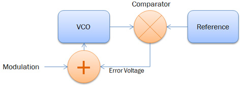
A simple PLL would just compare the frequency being produced by an VCO with some reference, determine the difference between the two, and if the two are different, provide an error voltage to the VCO to bring it back onto frequency. In the block diagram above, the error voltage is added to the modulation voltage as both of them affect the frequency of oscillation. This system would be great, and work a treat, if it was only necessary to operate on one frequency. However, if it is necessary to tune the VCO to different frequencies, some additional jiggery pokery is necessary.
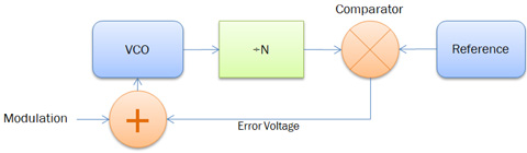
To make a tuneable PLL, an additional stage is added to the loop. The output from the VCO is divided by a number (let's call it 'N') and instead of having a reference frequency the same as the wanted output frequency, a much lower reference frequency is used. For example, if the reference frequency is 100 kHz, and we wanted the VCO to be on 89.6 MHz, we would divide the VCO output by 896 to give 100 kHz, and compare this to the 100 kHz reference. The rest of the circuit then operates as before. If we now change the division ratio to 900 instead of 896, the circuit would now attempt to retune the output to 90.0 MHz (assuming that the VCO was able to tune to that frequency). Thus, by changing the division ratio, we can lock the output frequency to any multiple of the reference frequency that we desire.
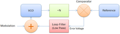
One difficulty of using a PLL in the case where we are trying to modulate the VCO (for example with audio or data) is that the PLL will see any modulation as a frequency error and try and correct it. To circumvent this problem it is normal to filter the error voltage produced by the PLL such that it cannot act upon the VCO at any frequency we are interested in modulating. If we are interested in audio frequencies which may descend as low as 20 Hz, we therefore need to low pass filter the error signal so that it cannot have any effect on modulation frequencies above 20 Hz and thus cannot try and 'correct' the audio being modulated onto the VCO.
This low pass filter is known as the loop filter. In addition to ensuring that the response of the loop is slow enough not to impact any low frequency modulation, it has the dual purpose of removing any of the reference frequency that might be present on the error voltage as the output of the comparator output will often just be a square wave whose mark-space ratio changes depending on the difference between the VCO frequency and the reference. If the required loop response time is slower than 20 Hz, and the reference frequency is 100 kHz this is not a difficult job, however having such a difference between the loop response time and the reference frequency leads to another difficulty: overshoot.
Imagine the situation...
- We switch on the PLL and the output frequency of the VCO is too low. The comparator recognises this and outputs a positive voltage to tell the VCO to increase its frequency. This positive signal is filtered by the loop filter which has the effect of slowing down the response time, and the VCO slowly begins to respond and its frequency rises.
- At some point the VCO output and the reference will now be the same and the comparator will stop producing a positive correction, however the loop filter, being very slow in comparison, has not yet finished acting upon its previous 'increase frequency' instruction and so instead of the PLL settling down, the output frequency continues to rise above the wanted one.
- The comparator now recognises that the frequency is too high and outputs a negative voltage to tell the VCO to reduce its output frequency. This instruction is slowed down by the laggard of the loop filter.
- Eventually the VCO output matches the reference and the comparator stops issuing its correction. But the loop filter has not yet finished the 'reduce frequency' instruction it was given and so the VCO frequency continues to go down.
- The comparator recognises this and outputs a positive voltage to tell the VCO to increase its frequency...
One solution to this is to speed up the loop filter response, but this would then mean that lower modulating frequencies would be corrected by the PLL. Another solution is to reduce the reference frequency so that the loop frequency and the reference frequency are sufficiently close that one does not lag the other too much. This, however, often means that the loop filter will not be able to filter out the comparator output sufficiently, leading to the reference frequency modulating the VCO and causing 'spurs' in the RF output that are separated from the VCO output by the reference frequency.
A common solution to the yo-yo problem is to use a 'lead-lag' filter instead of just a low-pass for the loop filter. A lead-lag filter is a low pass filter whose frequency response is flattened at some point in its frequency range. The advantage of this is that it can provide the filtering necessary to slow down the loop and get rid of the comparator output, whilst providing protection against the yo-yo-ing by having a flatter phase response. This can then be combined with a seperate filter to specifically remove the comparator output and together the two can ensure good performance and a clean VCO output.
add comment
( 425 views )
| permalink
| 
 ( 3.5 / 762 )
( 3.5 / 762 )
How not to design transmitters and receivers (part 3: RF matching)
Sunday 25 July, 2021, 20:31 - Amateur Radio, Broadcasting, Licensed, Pirate/Clandestine, Electronics, Radio Randomness
Posted by Administrator
Part 1 of this series investigated an oscillator to generate an RF signal, and Part 2 looked at output devices which can produce 1 Watt. In order to connect one to the other, an intermediate amplifier is usually required. This provides additional gain to make sure that the output device has enough drive and buffers the oscillator from any changes in the output load. There are plenty of transistors (including surface mount) that are capable of providing the necessary amplification, so this is easy. For the Wireless Waffle lockdown project, an MPSH10 transistor was used. This is capable of a around 150mW of output, has plenty of gain at VHF frequencies, is cheap, and is readily available. A surface mount equivalent (the MMBTH10) is also available if needed. Posted by Administrator
Easy right? Drive the input of the transistor from the oscillator, and connect it's output to the RF power device. Not quite so. The main difficulty is that the input impedance of the RF output transistor is very low, whereas the output impedance of the preceding amplifier is relatively high.
The output impedance of the intermediate amplifier can be calculated based on the output power it is required to deliver. The equation is as follows:
Rout = V2/2Po
where:
- Rout is the optimum load resistance of the amplifier.
- V is the Voltage swing at the output of the amplifier. This is generally the power supply voltage minus the voltage drop across the transistor when it is in operation.
- Po is the required output power in Watts.
How, then, to match a 300 Ohm output impedance to a 3 Ohm input impedance? Inter-stage impedance matching can be achieved either via transformers (which can offer broad bandwidth solutions), or by various arrangements of capacitors and inductors (which tend to need to be tuned around specific frequencies). The ratio of turns in a transformer is the square root of the ratio of the impedances, so in this case, a transformer would have to have a turns ratio of roughly 10:1. Such large impedance transformation ratios are difficult to achieve with transformers (for various as yet undiscussed reasons) and so an alternative approach is needed.
Impedance matching using basic networks made of inductors (L's) and capacitors (C's) can easily be done, however a simple two or three component network capable of converting from 500 to 3 Ohms would require a circuit with a minimum 'Q' factor of around 11. The Q factor determines the bandwidth of the network and roughly speaking if you divide the operating frequency by the Q, you get the half-power (3dB) bandwidth of the network. At 100 MHz for example, such a network would have a bandwidth of around 9 MHz, or put another way plus or minus 4.5 MHz from the centre frequency. This would work, but would clearly require re-tuning if the transmitter wanted to operate at different frequencies within the FM band, and as has been previously stated, any part that needs to be adjusted is subject to many potential failure modes.
So how's about a more complicated LC matching network? Calculating the necessary component values for LC matching networks with up to 4 components can be done relatively easily, and to make matters even more straightforward there is an online tool which will do it for you. The Impedance Matching Network Designer will do all the difficult sums. Just enter the input and output impedance you are trying to match and the web-site will do the necessary maths.
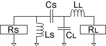 Entering 3 ohms and 300 ohms into the values for the load and source resistance respectively, results in a range of possible network topograhpies (fancy words which mean the relative positions of the L's and the C's). Some of these are more useful than others, and the one selected was the L-C-C-L network as depicted on the right. The values given by the calculator are as follows:
LS = 159 nH
CS = 17.6 pF
CL = 159 pF
LL = 14.3 nH
The advantage of this arrangement is that LS can be made the inductor which sits between the collector of the transistor and the power supply, providing it's power source and thus slightly reducing overall component count. Simulating this network using the excellent Micro-Cap tool (which is amazingly now free) from the appropriately named Spectrum Software and driving it directly from the collector of the MPSH10 showed a rather lumpy frequency reponse (shown below in blue - click for a larger version).;)
After some tweaking it was found that changing CS to 15 pF and CL to 180 pF, and adjusting LS and LL accordingly gave a better and less lumpy match between the two stages, and at the same time had sufficient bandwidth that no re-tuning of the network is needed across the frequency range 88 to 108 MHz (the red curve on the graph). This, incidentally, does not mean that changing the values can not give a better result. A 'broadband' matching network will almost always represent a compromise on the overall matching efficiency and playing around with the values can give additional gain on a particular frequency at the expense of a reduction in gain on a different frequency. However, as long as the output device and its driver have sufficient oomph to produce the required output across the whole frequency range, there is little to benefit from the extra gain. Of course, in real life, with actual (and not simulated) components the values may need further tweaking.

How not to design transmitters and receivers (part 2: RF power transistors)
Friday 16 July, 2021, 13:17 - Amateur Radio, Broadcasting, Licensed, Pirate/Clandestine, Electronics, Radio Randomness
Posted by Administrator
Any radio transmitter needs a final output device whose job is to deliver the required amount of radio frequency (RF) energy. For the purposes of the Wireless Waffle lockdown project, an output power of 1 Watt was determined to be sufficient for most purposes. Most purposes including:Posted by Administrator
- having fun by designing transmitters during lockdown;
- generating enough RF to leak signals around the house whilst connected to a dummy load;
- warming up a 1 Watt resistor to 'just about untouchable' heat levels;
- driving a higher power amplifier to several hundred watts for whatever purpose that might be used for.
Most modern RF power devices are based on various versions of a field effect transistor (FET). One of the complexities of using these devices (such as the RD01MUS1) is that they require a specific bias voltage on their gate in order to perform correctly. That would be all fine and dandy except for the fact that the aforementioned 'specific bias voltage' is different for each transistor. That's right, not for each type of transistor, but for each and every transistor. This is due to the manufacturing process of FETs and although this might be to tight tolerances, it still leaves the end device with sufficient variability that individual adjustment is required. The only way to get this right in a circuit is to manually set the bias voltage. This is usually done by monitoring the amount of current that the device is drawing without any RF passing through it and then adjusting the bias voltage until the current consumption is correct.
Although setting the correct bias voltage is a 'do once and walk away' kind of activity which doesn't need to be re-done once set, the need for any kind of variable component on a design is a nuisance for several reasons:
- Variable components (such as resistors or capacitors) are prone to age badly. Variable resistors, for example, often go open circuit due to the ingress of dust, or through corrosion.
- If the circuit is not working properly, there is a tendency to start fiddling around with anything that is variable, which could end up with a completely incorrect setting of the variable component.
- There is also a tendency to fiddle with anything variable to see if 'more power' can be generated. Whilst some settings may result in a higher output power they are also likely to reduce the life of the output device, or worse, blow it up due to excess current consumption.
The simplest alternative to the FET bias problem is to not use a FET. Bipolar junction transistors (BJT) are biassed very differently and do not succomb to the same problems. Instead they can be set up with no bias at all and what's more, this arrangement is perfect for amplifying constant signals (such as generated by an FM transmitter) and even has it's own name 'Class C'. The thing is that BJTs are decreasingly common for RF given many other (as yet undiscussed) factors which favour the use of FETs.
In the 1980s and 1990s, the 'go to' BJT for 1 Watt VHF transmitters was the 2N4427. This transistor would happily provide 1 Watt of output on most frequencies up to around 175 MHz and was relatively readily available and cheap. Manufacture of the 2N4427 ceased some years ago (some Chinese companies make a 'clone' which can provide 1 Watt at a push but is not the same device at all and is certainly not a drop-in replacement), and their availability and price are both becoming stretched. Whilst there are a number of equally aged transistors which can do a similar (or indeed a better) job, these too are no longer manufactured. A selection of these are listed below.
| Device | Output Power | Maximum Operating Frequency | Package | Gain |
|---|---|---|---|---|
| 2N6255 | 3 Watts | 175 MHz | TO-39 | 7.8 dB |
| 2SC730 | 1.5 Watts | 150 MHz | TO-39 | 10 dB |
| 2SC1947 | 4 Watts | 175 MHz | TO-39 | 10.5 dB |
| 2SC2329 | 2.5 Watts | 175 MHz | TO-39 | 13 dB |
| 2SC2131 | 1.6 Watts | 500 MHz | TO-39 | >7 dB |
| 2SC2851 | 0.9 Watts | 175 MHz | TO-92 | 13.5 dB |
| 2SC3017 | 2 Watts | 175 MHz | TO-39 | 11 dB |
| 2SC4767 | 0.9 Watts | 175 MHz | TO-92 | 13.5 dB |
| MRF227 | 3 Watts | 225 MHz | TO-39 | 13.5 dB |
| MRF237 | 4 Watts | 175 MHz | TO-39 | 12 dB |
| MRF555 | 1.5 Watts | 470 MHz | Power Macro | 11 dB |
| MRF607 | 1.8 Watts | 175 MHz | TO-39 | 11.5 dB |
| NTE472 | 1.8 Watts | 175 MHz | TO-39 | 11.5 dB |
| SD1127 | 4 Watts | 175 MHz | TO-39 | 12 dB |
| TP2314 | 3 Watts | 175 MHz | TO-39 | 15 dB |
Just about the only device being manufactured today which could theoretically replace the 2N4427 is the MRF4427 which, given it's name, is supposedly a surface-mount replacement for the original device, but which, like the Chinese clones, is not a drop-in replacement. It has a very different gain profile and works up to much higher frequencies. The secondary issue with the MRF4427 is that being a surface mount device, it is much more difficult to get rid of the heat which is generated in a transmitter. RF output devices are often no more than around 60-70% efficient, meaning that a 1 Watt output transistor will also be generating around half a Watt of heat. Whilst this is easily gotten rid of on a traditional transistor by sliding a heatsink onto it, it is much more difficult to get rid of with a surface mount device (SMD). There are heatsinks available for surface mount devices but these are typically 'glued' onto the device which, though it may work, is not a perfect way. Better, perhaps, might be to try and get rid of the heat by distributing it around the printed circuit board (PCB).
;) 2N4427 (TO-39) | ;) 2SC2851 (TO-92) | ;) MRF555 (Power Macro) |
For standard, double sided, FR4 PCB material, the thermal characteristics of the PCB are such that it will rise around 500°C per Watt per square centimetre of board. Copper via's between the top and bottom of the board can help reduce this. Dissipating a half Watt of heat in a centimetre square of PCB will therefore raise the temperature of the PCB by up to 250°C which is far too hot a temperature for any transistor to operate. However, if the transistor is mounted on a bigger piece of PCB, the heat will be distributed over a wider area and it becomes possible to get rid of half a Watt of heat without being left with a device whose main purpose would be boiling tin.
 Given all the above, for the Wireless Waffle lockdown project, after scouring the planet for sources of 30 year old transistors, the decision was eventually made to use an MRF555 device. This has nice, healthy sized leads which can be soldered onto pads on a PCB and the heat will be distributed across the PCB from all four pins of the device. It's still readily available (though no longer manufactured), relatively cheap, and being a device designed for UHF use, it loafs along at VHF frequencies, making it more efficient and therefore producing less heat. When mounted on a PCB, producing a Watt of RF, it heats up to around 65°C which is hot to the touch, but won't damage the device (or your skin too badly if you touch it).
 How not to design transmitters and receivers (part 1: voltage controlled oscillators)
Saturday 5 June, 2021, 12:20 - Amateur Radio, Broadcasting, Licensed, Pirate/Clandestine, Electronics, Radio Randomness
Posted by Administrator
Posted by Administrator
 Hasn't lockdown been a bore? There is only so much Netflix or Amazon Prime that it's possible to watch, let alone enjoy. Mind you, having said that, and if you haven't already seen it, Halt And Catch Fire is a must-watch for any kind of nerd or geek who remembers the dodgy, unreliable and overheating computer designs of the early 1980s.
In order to maintain some kind of sanity, in the Wireless Waffle workshop work has been proceeding on the crudely conceived idea of an instrument that will not only supply emissions for use in radio transmissions, but one which would also be capable of receiving them. Or to put it simply, a wideband VHF transmitter and a matching receiver which could be used as an audio link. Having designed and built many of these devices back in the 1990s, it ought to have been relatively straightforward to revisit those designs and modernise them. Alas, RF design is a fickle mistress and in addition to resulting in some truly awful designs, some very nice ones have also emerged. Along the way, many topics have had to be re-learnt all of which makes for some (very techy) content for a series of blog posts which may, in some small way, help those who might seek to replicate this pointless pass-time.
As Julio Iglesias once said, let's Begin (at) The Beg(u)in(e)(ning). There are dozens of designs for simple VHF variable frequency oscillators (VCO) on the internet, so getting something to generate the intial signals ought to be relatively straightforward. However, there is also lots of evidence to suggest that in cases where signals from oscillators are amplified to high power levels, and sent through antennas which are relatively close to the transmitter, radio frequency (RF) feedback can occur causing buzz and hum to the transmitted signal. The way around this is to have the oscillator work on a different frequency to the one being transmitted.
This might seem like an odd thing to do, however it is not uncommon. Two primary methods are used to achieve this:
- A variable oscillator is mixed with a fixed oscillator and the sum (or difference) of the two is then filtered and amplified. For example, a variable oscillator covering 100 to 125 MHz could be mixed with a fixed oscillator at 75 MHz, resulting in outputs either at 175 to 200 MHz (if the two signals are added) or 25 to 50 MHz (if the two are subtracted). The difficulty with this approach is that mixers are, almost by necessity, non-linear devices. In the first case, with the oscillator on 100 MHz, and the wanted output on 175 MHz, the second harmonic of the oscillator would fall at 200 MHz which, being within the 'wanted' output range, could not easily be filtered out. Careful selection of the variable and fixed frequencies can help overcome this, however this limits the possible range of output frequencies and also requires lots of filtering which is fine if the wanted frequency range is relatively narrow, but more difficult if the frequency range is wider.
- The varible oscillator operates at a frequency which is a sub-harmonic of the wanted frequency, and a multiplier is then used to double, triple or multiply the frequency by even higher orders. If we therefore wanted an output from 25 to 50 MHz, we could, for example, use an oscillator running from 8.33 to 16.66 MHz and triple it. Once again, multipliers are also non-linear devices and the 16.66 MHz signal would also be doubled to 33.33 MHz, which being within the wanted output frequency range would also be difficult to filter out. This method therefore is not without its problems and also requires filtering with all the issues associated with that.
Digging around the internet for 'Kalitron' circuits in which the double frequency (or '2f') output is available, yielded very few results. An article entitled, High Frequency VCO Design and Schematics by Iulian Rosu did discuss a Differential Cross-Coupled VCO and though Iulian's design is meant for very high frequencies, his article does provide some useful guidance. One of these is that the transistors should ideally be biased at the point between their saturation and linear regions (i.e. almost fully turned on). It was therefore decided to try and adopt this circuit.
Since getting involved in designing radio equipment in the 90s, the use of PNP transistors for oscillators has always been the preferred Wireless Waffle approach. The primary benefit of this is that the inductor used to set the frequency of the oscillator is grounded, making applying some kind of variable capacitance across it far easier. And so experimentation began. It would have been easy to copy the Veronica approach, however this requires 6 individual coils to be wound, and finding a simpler way to achieve the same results was sought. Getting such an oscillator to work was not difficult, but finding the correct balance of transistor current and bias, and then tapping off the doubled frequency component with sufficient 'oomph' to do something useful with, whilst not disturbing the oscillator's stability proved a complex balancing act. In addition, to keep the costs of the associated (and yet to be designed) phase locked loop (PLL) down by using off-the-shelf high speed CMOS chips also required a method to extract the un-doubled output to be found.
The final design works. Actually, that was meant to be the start of a sentence, but having got as far as 'the final design works', seemed sufficient.
;) An inductor wound on a toroidal core was used for the oscillator, with a secondary winding (not shown in the picture) used to tap off the un-doubled output. This is somewhat fiddly to wind, but with practice becomes much easier and is the alternative to winding the 6 coils used in the Veronica design.
An inductor wound on a toroidal core was used for the oscillator, with a secondary winding (not shown in the picture) used to tap off the un-doubled output. This is somewhat fiddly to wind, but with practice becomes much easier and is the alternative to winding the 6 coils used in the Veronica design.Once oscillating a new issue was identified: the varicap diodes being used to tune the circuit were rectifying the RF generated by the circuit causing mountains of unwanted non-linear signals to be generated. This was partially fixed by not connecting the varicaps directly together but by short-circuiting them at RF with a capacitor whilst driving the DC level through separate resistors. Keeping the drive voltage above around 4 Volts keeps the diodes in their non-rectifying, more linear region though slightly reducing the potential tuning range. Reducing the amplitude of the oscillations would solve this a little but also reduce the potential output power. RF design is nothing if not a set of complicated compromises.
The doubled output from the oscillator is around 10 dBm (10 milliWatts) which is not quite enough to immediately drive a power amplifier to a reasonable level, so a buffer will be needed. The addition of a buffer will add (at a later date) the option to implement an 'out of lock power down' function in which the output of the transmitter is switched off until it has settled on the required frequency, without which a multitude of problems can occur.
The final circuit (or 'schematic' in American English) of the voltage controlled frequency-doubling oscillator (or 'uppy-downy-frequency-makey-matey' in Australian English) is shown below. Layout should be kept as symmetric as possible to minimise the amount of 'f' which is present on the '2f' output. The transistors used were originally type BF451 which are ideal for the task but other PNP RF transistors such as the BF509, BF939 or MPSH81 would work equally well.
;)
Future articles in this series may explore other unbelievably exciting topics such as:
- how not to blow up RF power transistors
- how well soldering irons burn things like skin and phone covers
- why 40 year old transistors trump modern ones
- glaringly obvious mistakes to make when sending PCBs for production
- forgetting that receivers are sensitive devices
- badly matching one stage to another
- getting PLL loop filters to oscillate wildly
- and much, much less...