
How not to design transmitters and receivers (part 8: divide by N)
Friday 3 September, 2021, 08:46 - Amateur Radio, Broadcasting, Licensed, Pirate/Clandestine, Electronics
Posted by Administrator
The next functional block that is required to complete a transmitter (not a receiver for which there are many other blocks to consider) is the 'divide by N' device. In principle, all that is required to achieve this function is a counter which will count up (or down) until it reaches a particular number (or zero), indicate this (i.e. with some kind of output pulse) and reset itself. Posted by Administrator
There are many ways of achieving this from the use of logic ICs to dedicated counter ICs. Let's begin with the logic IC approach. Any binary counter which has a way of being reset to zero can be used as a counter. It's simply a matter of detecting when the right combination of bits have reached '1' and then resetting the counter and starting again. A simple way of doing this is using a CMOS 4020, 4024, 4040 or 4060 counter. To check when a selected number of bits are all 1's, connect the cathode of a number of diodes to the relevant bits, connect the anodes together to a common point and then join that point to positive via a suitable resistor. When any of the bits are zeros, they will pull the common point down to ground through the diodes. Only when all of the bits are 1's will the common point go high. An example circuit, including a switch to decide which diodes (and thus which bits) are tied to the common point is shown to the right (click for a larger version).
;) Pin 11 of the 74HC4020 counter is connected to the positive supply by the 2.2K resistor, and will reset the counter to zero when it goes high. However, this is the common point for the diodes which will pull this point down to ground when any of the bits of the counter switched into circuit are zero. Only when all the bits which are switched into circuit go high will pin 11 go high, at which point the counter resets and will start counting again at the next input clock pulse. The output of the circuit could be taken from the common point, however the reset pulse is very narrow and may be missed by, for example, a slower operating phase comparator. In this example, the output is taken from the second most significant bit, which will give something nearer to a square wave. Note that the diodes have been arranged so that the switches are in binary significance order with the most significant bit being on the right hand side and the least on the left.
Pin 11 of the 74HC4020 counter is connected to the positive supply by the 2.2K resistor, and will reset the counter to zero when it goes high. However, this is the common point for the diodes which will pull this point down to ground when any of the bits of the counter switched into circuit are zero. Only when all the bits which are switched into circuit go high will pin 11 go high, at which point the counter resets and will start counting again at the next input clock pulse. The output of the circuit could be taken from the common point, however the reset pulse is very narrow and may be missed by, for example, a slower operating phase comparator. In this example, the output is taken from the second most significant bit, which will give something nearer to a square wave. Note that the diodes have been arranged so that the switches are in binary significance order with the most significant bit being on the right hand side and the least on the left.This circuit works very well, however it has one minor flaw and one major, yet surmountable one. The minor flaw is that a finite amount of time is required between the common point going high and the counter being reset. This time is measured in nanoseconds, however if the counter is running particularly quickly (i.e. at frequencies measured in MHz where each bit is less than a microsecond long) this delay means that the counter counts to 'N and a bit', the 'bit' being the extra time taken for the counter to reset. Some circuits set the counter to 1 less than is required, and use an additional flip-flop to count the last bit whilst giving the counter time to reset, but this adds extra complexity (and thus cost) to what is an otherwise simple circuit.
The major yet surmountable flaw is that each output pin of the divider has a square wave on it. These pins generate small but nevertheless detectable harmonics right across the radio spectrum. If a prescaler is noisy, these things are deafening and as receivers are very sensitive, these outputs will produce interfering signals at almost any and every frequency to which you may wish to tune unless extreme care is taken to shield this part of the circuit from the receiver parts. Thus, whilst such a design is great in a transmitter (assuming a buffer and/or prescaler is used between the VCO and it), it is a veritable pain in the back-side in a receiver.
There are, thankfully, a number of pre-settable counters which overcome both of these problems. An old device but one which is very easy to use and understand is the TC9122P.
;)
The TC9122P can count from 1 to 3999 and its inputs are in binary blocks of 10 (otherwise known as binary coded decimal, BCD). So to divide by 896 or 1079, the required setting would look something like:
| 0 | 8 | 9 | 6 | 1 | 0 | 7 | 9 | |
| 00 | 1000 | 1001 | 0110 | 01 | 0000 | 0111 | 1001 |
;) Rotary BCD switches are available which could be directly connected to the inputs and then frequencies could simply be 'dialled' in. The same result can also be achieved with a 4059 which is a little more complicated as it has a number of different counting modes including, though, BCD. An example of using BCD switches to dial up a frequency is illustrated on the left (which is taken from a Broadcast Warehouse 1 Watt FM exciter).
Rotary BCD switches are available which could be directly connected to the inputs and then frequencies could simply be 'dialled' in. The same result can also be achieved with a 4059 which is a little more complicated as it has a number of different counting modes including, though, BCD. An example of using BCD switches to dial up a frequency is illustrated on the left (which is taken from a Broadcast Warehouse 1 Watt FM exciter).In part 7 of the 'How not to design transmitters and receivers' the MC145151 was introduced. This IC includes a divide by N counter which is a straightforward binary (and not BCD) counter. One oddity with that particular chip is that the input pins to the counter are tied high with an internal resistor meaning that pins which need to be set to zero should be connected to ground, whereas with many other counters it is usually the pins which need to be set to one which should be connected to positive.
An example of using standard binary to set the numbers 896 and 1079 are shown in the table below.
| Decimal | Binary |
|---|---|
| 896 | 01110000000 |
| 1079 | 10000110111 |
One thing that was noticed when considering using straight binary (and not BCD) for programming frequencies across the FM band is that to select numbers over 1023 (e.g. if using a reference frequency of 100 kHz and wishing to access the whole FM band such that numbers up to 1079 are required), 11 binary digits are required (that's eleven, not three). Nice, cheap, binary switches are available in 10 or 12 bit versions. Whilst it would have been easy enough to use a 12 bit switch and leave one bit unused, it would be even nicer to find a way to use a 10 bit switch.
 Such a way was found. If we call the most significant bit 'bit 11' then bits 9 and 10 can be tied together (as has actually been done in the counter circuit above). This means that any binary number from '01100000000' representing 768, to '10011111111' representing 1279 can be set. Assuming a 100 kHz reference frequency, anything from 76.8 to 127.9 MHz can be set using just a 10 bit switch. In addition (though potentially rather uselessly in this application) any other binary number in which bits 9 and 10 are the same can also be selected. Thus numbers from '00000000000' (0) to '00011111111' (255) and '11100000000' (1792) to '11111111111' (2047) could also be set, potentially representing frequencies from 0 to 25.5 and 179.2 to 204.7 MHz.
We now have nearly all the blocks necessary to create a variable frequency phase lock loop based FM transmitter. There's still the reference oscillator (which is relatively trivial) and low pass filtering to go.
add comment
( 137 views )
| permalink
| 
 ( 2.2 / 459 )
( 2.2 / 459 )
How not to design transmitters and receivers (part 7: phase comparators)
Wednesday 1 September, 2021, 08:31 - Amateur Radio, Broadcasting, Licensed, Pirate/Clandestine, Electronics
Posted by Administrator
One of the blocks yet to be discussed in the Wireless Waffle lockdown transmitter and receiver project is the phase/frequency comparator. In days of yore (a.k.a. the 1980s), the go-to integrated circuit (IC) for this function was the trusty 4046. This not only contains a couple of different types of phase comparator (the newest versions have three, the older ones just two) it also has a built in voltage controlled oscillator (VCO). The VCO works well up to a few MHz, or even higher depending on the specific type of IC, but is useless at VHF and thankfully can be easily inhibited. As, however, the phase comparator only needs to work at the reference frequency (usually a few kHz), the 4046 will function perfectly well in this role.Posted by Administrator
The 4046 takes the reference input on pin 14 (oddly termed the 'signal in' pin) and the variable frequency input on pin 3 (the 'comparator in'). The two phase comparator outputs are on pins 2 ('comparator I output') and 13 ('comparator II output'). On newer versions a third phase comparator output can be found on pin 15; on the older versions pin 15 has a Zener diode connected to it which is intended to be used to stabilise the power supply when using the VCO but was almost never employed.
;)
The Type I phase comparator is just an XOR gate. This produces a square wave output whose mark-space ratio varies with the difference in phase of the inputs. This can be fed into a loop filter to yield a voltage which varies up or down with the difference in phase. The primary difficulty with this method is that both the reference frequency, and the variable frequency input must be square waves with equal mark-space ratios. For the reference which is usually a square wave divided down from some crystal oscillator, this is usually not a problem, however the signal from the oscillator, following its traversal through the 'divide by N' circuit, is often just a pulse. Many divide by N devices just count a specific number of times, and when that count has been reached output a brief pulse. Additional circuitry is required to turn this into a square wave.
The Type II phase comparator is an altogether more sophisticated device and as well as not caring about the mark-space ratio of the two input signals, produces a positive 'up' or negative 'down' signal at its output instead of just a square wave. If its output is connected to a capacitor (through a suitable current limiting resistor) the voltage across the capacitor will only be given a push up or down if the phase of the input signals is different. If the two are fully in phase, the output of the Type II detector is an open circuit. This massively reduces the amount of the reference frequency that appears at the input to the loop filter, making the whole PLL output cleaner. When modulating the VCO, there will almost inevitably be occasional phase differences so the output will rarely be totally quiet, but this type of detector is generally far easier to work with.
Most modern PLL ICs have a reference oscillator and divider, the divide by N counter, and the phase comparator functions included in them in a single package. Some even have built-in prescalers. Even some older devices integrate several of these functions. The MC145151 which was commonly used in many of the CB radios of the 1980s contains all except the prescaler. The phase detector in this device is akin to the Type II device in the 4046 but has two separate outputs:
- a single pin output mimics the operation of the 4046, with positive and negative pulses and an open circuit when the reference and VCO are in phase, and
- seperate 'up' and 'down' pins which need to be fed into an external combiner/loop filter to generate the voltage to feed the VCO.
;)
How, then, to get a bigger voltage swing? One method would be to feed the output from the phase comparator into an op-amp with a higher supply voltage, and set up with a gain profile which steps up the 5, 9, 12 or whatever voltage is available from the phase comparator to a higher value. The circuit pictured above will do this. The input from the phase comparator first goes through the previously discussed 'lead-lag' low pass filter. The op-amp is set to have a gain of 2.4, so that a 5 Volt input will give a 12 Volt output. This amplifier, as well as increasing the voltage swing will also, however, amplify any noise at the output of the phase comparator and thus is not ideal.
This is where the seperate 'up' and 'down' pin output of devices such as the MC145151 come into their own. Given that there has got to be an external loop filter to use these outputs, this could by default run from a higher supply voltage. Also, as the signals are only nudges up or down, the active loop filter that follows would not further amplify any noise generated by the phase comparator.
;)
The circuit above gives an example of this and has a similar frequency response to the earlier amplifier circuit. It has has a differential input: A positive nudge on the 'V up' input will cause the output voltage to rise and similarly a positive nudge on the 'V down' input will cause the output voltage to fall. When both are silent, the output voltage will hold steady. In this steady state, no noise is being generated or amplified making this kind of approach relatively quiet.
Of course in most cases a 30 Volt supply won't be available (though one could be generated using a simple charge pump but that's for another day), however supplying the amplifier and thus the VCO from even a 12 Volt supply will give an improved frequency range compared to 5 or 9 Volts.

How not to design transmitters and receivers (part 6: prescalers)
Wednesday 25 August, 2021, 09:39 - Amateur Radio, Broadcasting, Licensed, Pirate/Clandestine, Electronics, Radio Randomness
Posted by Administrator
Part 5 of the series 'How not to design transmitters and receivers' discussed phase locked loops (PLL) and the fact that programmable dividers (divide by 'N') are required in order to make a PLL which can operate on different frequencies. Such a divider would need to be able to take radio frequency (RF) signals at its input before doing the dividing. Off-the-shelf CMOS logic chips in the 74HC series are generally capable of operating at frequencies up to 50 or 60 MHz (and in some cases up to 70 MHz). These could therefore be directly used as dividers in low frequency circuits where a solid 5 Volt signal can be fed into them, but anything operating at over about 70 MHz, or which produces a smaller output, requires some other technology.Posted by Administrator
This is then the realm of the 'prescaler'. A prescaler is basically a high frequency divider, often with a fixed division ratio, or in some cases with a limited number of fixed ratios. In most cases they are also designed to accept a low-level RF input rather than needing 5 Volts peak-to-peak.
There are an enormous number of prescaler IC's available, some dating back to the early 1980s. Thankfully, a useful look-up table of prescaler specifications is available online. The requirements for the Wireless Waffle lockdown project are that the prescaler must meet the following specifications:
- Be able to operate at frequencies down to around 25 MHz (so that the half-frequency oscillator can be used in Band-I, i.e. around 50 MHz, if needed).
- Be able to operate at frequencies up to around 600 MHz (so that future UHF designs can use the same chip).
- Have a division ratio of at least 40 (so that a 600 MHz input will be brought well within the frequency range of other digital components).
- Accept a reasonable and if possible wide range of input powers (to simplify the design of any circuitry feeding it).
- Be reasonably cheap (of course!)
- Be relatively widely available (so that there won't be any problems in getting hold of any for future projects).
To find a suitable device, it was necessary to carefully peruse the exact specification sheets of various devices. Most have a 'guaranteed operating range' which is the combination of input frequency and input power over which they will perform perfectly. However, the specification sheets often contain performance curves which show input power and input frequency combinations that should work fine but are not guaranteed. A number of prescalers have guaranteed operating ranges which go as low as 50 or 70 MHz, but the datasheet shows that they will operate below this range, generally if they are driven with slightly higher input power.
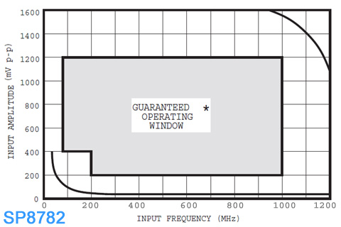
Take, for example, the above chart taken from the datasheet for an SP8782 prescaler. The guaranteed operating window covers the frequency range from 200 MHz to 100 MHz with an input level of 200 mV peak-to-peak, descending to around 50 MHz (according to the datasheet, though the chart makes this look more like 70 MHz) if the input level is increased to 400 mV. However, even lower and higher frequency performance is possible. In the case of lower frequencies, it would appear to operate down to as low as maybe 25 MHz and as high as 1200 MHz if the input levels are suitably adjusted.
Slight aside: The MB501 requires a 2K (or thereabouts) pull-down resistor on its output to function. This isn't optional, it's mandatory. It's easy to forget this and wonder why the circuit isn't working...!
After much research, the MB501L was selected for the Wireless Waffle project. This has a guaranteed minimum operating frequency of 10 MHz, a maximum of 1100 MHz, and over this range will perform correctly with an RF input ranging from -4 to +6 dBm (1 milliWatt give or take). It has a pre-settable division ratio of 64, 65, 128 and 129. What's more one can be bought online for around £1.50 and seems relatively widely available despite originally being of mid 1980s vintage.One other thing to consider when using prescalers is that they often do a rather bad job of isolating their inputs from their outputs (and their power supply rails). This means that the divided signal can easily get into whatever they are connected to, and in particular the RF inputs, causing spurs on the RF signal at multiples of the divider output. Take an example of a 64 MHz oscillator, connected to a device such as the MB501L set to divide by 64. The output frequency of the divider will be 1 MHz, and if care is not taken, this will find its way back into the oscillator meaning that unwanted spurs 1 MHz from the oscillator (i.e. at 63 and 65 MHz) will be produced.
Solutions to this include a buffer between the oscillator and the prescaler, or the introduction of sufficient loss (i.e. through a resistor) between the two to minimise the impact of any lack of isolation in the prescaler. Unless there is an excess of RF power to play with, the best option is to use a buffer. There are a myriad of RF buffer schematics online to choose from. In this application, one of the main criteria is the amount of isolation between input and output as this is the purpose to which the buffer is being put. Another design criteria is for the buffer to produce the right level of output to drive the prescaler at its preferred input levels. Field effect transistor (FET) buffers are particularly good when it comes to input/output isolation, and a very simple buffer can be constructed with the minimum of components. Bipolar transistors (BJT) can also be used, but tend not to have such good isolation. Two such buffer circuits are presented below.
;)
The Junction-FET (JFET) circuit has a very high input impedance (largely set by the value of the 220K resistor from its gate to ground) and good isolation. The input impedance of the BJT circuit will be much lower and isolation poorer, so what, you might ask, is the benefit of the BJT approach. The answer is simple: some companies who manufacture printed circuit boards (PCBs) can also assemble surface mount devices (SMD) on the board at very low prices, and the 2SC3356 shown in the schematic is a device which these manufacturers have in their low-cost stock room, whereas they rarely have JFETs available.
At this point we nearly have all the building blocks necessary to make a fully synthesised transmitter bar a couple - the 'divide by N' block, and the 'phase/frequency comparator'. More, then, to follow soon.
How not to design transmitters and receivers (part 5: phase locked loops)
Thursday 12 August, 2021, 09:39 - Amateur Radio, Broadcasting, Licensed, Pirate/Clandestine, Electronics, Radio Randomness
Posted by Administrator
Parts 1 to 4 of this series have covered generating an RF signal, amplifying it, and providing the whole kit and caboodle with a nice clean power supply. In this part, we consider frequency stabilisation.Posted by Administrator
It is very straightfoward to produce a radio frequency (RF) signal that does not drift from the wanted frequency. Using a quartz crystal oscillator, it is possible to maintain an accuracy of a few parts per million, or a couple of Hz per MHz of output frequency. However, the output from a crystal is so stable that it's just about impossible to move it. If you want to modulate the frequency by more than a few kHz, using a crystal is therefore not feasible. For a wideband FM transmitter, where the required deviation (i.e. the amount by which the frequency changes) is +/- 75 kHz, using a crystal is therefore a non-starter. Instead it is necessary to use a voltage controlled oscillator (VCO) and surround this by some kind of feedback loop which samples the output frequency and corrects it if it has drifted off the wanted frequency. Such a feedback loop is called a phase locked loop or PLL (or indeed a frequency locked loop).
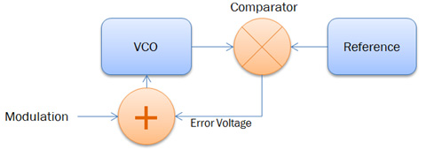
A simple PLL would just compare the frequency being produced by an VCO with some reference, determine the difference between the two, and if the two are different, provide an error voltage to the VCO to bring it back onto frequency. In the block diagram above, the error voltage is added to the modulation voltage as both of them affect the frequency of oscillation. This system would be great, and work a treat, if it was only necessary to operate on one frequency. However, if it is necessary to tune the VCO to different frequencies, some additional jiggery pokery is necessary.
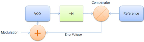
To make a tuneable PLL, an additional stage is added to the loop. The output from the VCO is divided by a number (let's call it 'N') and instead of having a reference frequency the same as the wanted output frequency, a much lower reference frequency is used. For example, if the reference frequency is 100 kHz, and we wanted the VCO to be on 89.6 MHz, we would divide the VCO output by 896 to give 100 kHz, and compare this to the 100 kHz reference. The rest of the circuit then operates as before. If we now change the division ratio to 900 instead of 896, the circuit would now attempt to retune the output to 90.0 MHz (assuming that the VCO was able to tune to that frequency). Thus, by changing the division ratio, we can lock the output frequency to any multiple of the reference frequency that we desire.
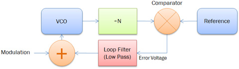
One difficulty of using a PLL in the case where we are trying to modulate the VCO (for example with audio or data) is that the PLL will see any modulation as a frequency error and try and correct it. To circumvent this problem it is normal to filter the error voltage produced by the PLL such that it cannot act upon the VCO at any frequency we are interested in modulating. If we are interested in audio frequencies which may descend as low as 20 Hz, we therefore need to low pass filter the error signal so that it cannot have any effect on modulation frequencies above 20 Hz and thus cannot try and 'correct' the audio being modulated onto the VCO.
This low pass filter is known as the loop filter. In addition to ensuring that the response of the loop is slow enough not to impact any low frequency modulation, it has the dual purpose of removing any of the reference frequency that might be present on the error voltage as the output of the comparator output will often just be a square wave whose mark-space ratio changes depending on the difference between the VCO frequency and the reference. If the required loop response time is slower than 20 Hz, and the reference frequency is 100 kHz this is not a difficult job, however having such a difference between the loop response time and the reference frequency leads to another difficulty: overshoot.
Imagine the situation...
- We switch on the PLL and the output frequency of the VCO is too low. The comparator recognises this and outputs a positive voltage to tell the VCO to increase its frequency. This positive signal is filtered by the loop filter which has the effect of slowing down the response time, and the VCO slowly begins to respond and its frequency rises.
- At some point the VCO output and the reference will now be the same and the comparator will stop producing a positive correction, however the loop filter, being very slow in comparison, has not yet finished acting upon its previous 'increase frequency' instruction and so instead of the PLL settling down, the output frequency continues to rise above the wanted one.
- The comparator now recognises that the frequency is too high and outputs a negative voltage to tell the VCO to reduce its output frequency. This instruction is slowed down by the laggard of the loop filter.
- Eventually the VCO output matches the reference and the comparator stops issuing its correction. But the loop filter has not yet finished the 'reduce frequency' instruction it was given and so the VCO frequency continues to go down.
- The comparator recognises this and outputs a positive voltage to tell the VCO to increase its frequency...
One solution to this is to speed up the loop filter response, but this would then mean that lower modulating frequencies would be corrected by the PLL. Another solution is to reduce the reference frequency so that the loop frequency and the reference frequency are sufficiently close that one does not lag the other too much. This, however, often means that the loop filter will not be able to filter out the comparator output sufficiently, leading to the reference frequency modulating the VCO and causing 'spurs' in the RF output that are separated from the VCO output by the reference frequency.
A common solution to the yo-yo problem is to use a 'lead-lag' filter instead of just a low-pass for the loop filter. A lead-lag filter is a low pass filter whose frequency response is flattened at some point in its frequency range. The advantage of this is that it can provide the filtering necessary to slow down the loop and get rid of the comparator output, whilst providing protection against the yo-yo-ing by having a flatter phase response. This can then be combined with a seperate filter to specifically remove the comparator output and together the two can ensure good performance and a clean VCO output.