
How not to design transmitters and receivers (part 10: varicaps)
Tuesday 14 September, 2021, 08:45 - Amateur Radio, Broadcasting, Licensed, Pirate/Clandestine, Electronics
Posted by Administrator
Before heading down the final straight of the Wireless Waffle lockdown transmitter project, and mounting the horse of the associated receiver, a few words on varicap diodes, or varactors as they're also known. Posted by Administrator
A varicap is a diode which, when reverse biassed (i.e. not conducting) acts as a capacitor. Varying the voltage of the reverse bias, affects the amount of capacitance that the device exhibits. The higher the reverse voltage, the smaller the capacitance. These, are therefore the devices which enable an oscillator's frequency to be tuned with a voltage. Replacing the capacitor in a tuned circuit with a varicap allows the resonant frequency (and thus the frequency of oscillation) to be varied, making a voltage controlled oscillator (VCO).
However, not all varicaps are made the same. The amount of capacitance they exhibit can be very different. Some are designed for use in medium-wave circuits and can have several 100pF of capacitance. Some are designed for UHF and have only a few picoFarads (pF) of capacitance. Some operate only over a relatively narrow range of voltages, some require a very wide range of voltages to perform to their best. There are also differences in the extent to which the capacitance changes between a low reverse voltage and a high one. Some varicaps will have 10 or more times less capacitance at a high voltage compared (say 28 Volts) to a low one (say 1 Volt), whereas others may only have a high to low capacitance ratio of nearer 4.
For use in a VHF VCO being discussed in this series, a varicap with a capacitance varying from around 20pF to 10pF would be about right. Paired with an inductor of around 120nH and together with the stray capacitances of the oscillator circuit, this will enable oscillation over the frequency range of interest. To resonate a 120nH coil at 87.5 MHz requires a parallel capacitance of 27.5pF, falling to 18pF at 108 MHz. So a varicap which can tune from 20pF to 10pF in parallel with around 8pF of stray capacitance would be spot on.
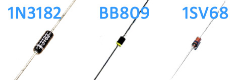
There are a wide range of varicap diodes which can perform this job, and an equal number which can't. Trying to find data online for some devices can prove very difficult as many which are cheaply available are of a vintage where few datasheets remain, and some are originally of Japanese manufacture meaning that the datasheets are primarily in Japanese. Below is as many devices as have been found which ought to be able to do the job in hand. Note that all of these devices are in a two lead, glass-body package (such as the good old 1N4148). There are surface mount devices (SMD) available, and some odd square packages but these have not been listed, due to their lack of aesthetic pleasure-giving.
| Device | Specified Use | Maximum Capacitance and Voltage | Minimum Capacitance and Voltage |
|---|---|---|---|
| BB139 | VHF Tuner | 29pF@3V | 6pF@30V |
| BB329 | VHF & CATV Tuner | 35pF@1V | 3pF@28V |
| BB409 | VHF Tuner | 27pF@3V | 6pF@25V |
| BB609 | VHF & CATV Tuners | 33pf@1V | 3pf@28V |
| BB809 | VHF Tuners (up to 160 MHz) | 42pF@1V | 4.5pf@28V |
| BB909 | VHF Tuners (up to 460 MHz) | 24pF@1V | 3pf@28V |
| 1N3182 | VHF Tuning | 33pf@4V | ? |
| 1S2688 | VHF AFV | 20pF@1V | 2.2pf@10V |
| 1SV68 | VHF/FM Tuner | 32pf@3V | 5pF@25V |
| 1SV97 | VHF Tuning | 25pf@?V | ? |
| 1SV113 | VHF Tuning | 21pF@3V | 3pf@25V |
| 1SV124 | VHF Tuning | 35pF@1V | 3pF@28V |
| 1SV126 | FM/VHF Tuning | unknown | |
| 1SV155 | VHF Tuning | unknown | |
| 1SV184 | FM/VHF Tuning | 50pf@2V | 4-6pf@10V |
Incidentally, if anyone knows of any other devices which can do the job, please post them in the comments and they can be added to the table. Also, if anyone has the precise details of any of the diodes whose parameters are 'unknown', any information on them would be greatly received.
In the VCO design presented in part 1 of this series, two varicaps are used in a back-to-back arrangement. It is important that these two are relatively well matched. Some of the older diodes listed above (such as the BB139 or 1N3182) are not well matched, and the datasheet shows that the exact capacitance value provided at a particular voltage can be as much as 30% different between two devices. This either means measuring and selecting two similar diodes or choosing more modern components whose tolerances are much better. Of course more modern devices are often more expensive, so like many things, there's a trade-off to be had.
add comment
( 195 views )
| permalink
| 

 ( 2.6 / 542 )
( 2.6 / 542 )
How not to design trasmitters and receivers (part 9: low-pass filters)
Monday 6 September, 2021, 15:41 - Amateur Radio, Broadcasting, Licensed, Pirate/Clandestine, Electronics
Posted by Administrator
Many designs for transmitters and power amplifiers which can be found online (certainly some of the older designs such as the one below) fail to include any low pass filtering on their outputs. Posted by Administrator
;)
There are several possible reasons for this:
- maybe it was expected that the avid constructor would know to add their own filter;
- maybe it was thought that any antenna connected to the device would magically filter out the harmonics (actually, this can sometimes happen for even multiple harmonics such as the 2nd, 4th and 6th, but is not the case for the odd ones);
- maybe (for older designs) there was such light use of radio frequencies that it didn't matter if your transmitter also radiated on a bunch of other frequencies.
| Harmonic | Frequencies | Services |
|---|---|---|
| 2nd | 175 - 216 MHz | DAB Radio, PMR |
| 3rd | 262.5 - 324 MHz | Military Aircraft |
| 4th | 350 - 432 MHz | Military Aircraft, Blue Light Communications, Emergency Distress Beacons, PMR, Radio Amateurs |
| 5th | 437.5 - 540 MHz | Radio Amateurs, PMR, Television |
Of course the specific frequency of operation will determine exactly which service may be affected. It's not as if a transmitter produces harmonics on all these frequencies simultaneously. However there are some bad options within this range. Imagine a transmitter on the roof of a building where there is a DAB receiving antenna, the 2nd harmonic of the transmitter could wipe out DAB reception, causing annoyance to those trying to listen to the extremely poor quality, low bit-rate audio services that DAB provides. Even worse is the 3rd harmonic. There is no way in which you want to be tracked down by the military for interfering with their aeronautical communications and, as previously mentioned, something like a simple dipole will radiate perfectly well at the 3rd harmonic as well as the fundamental frequency.
The solution is to fit a filter at the output of the transmitter. The purpose of this filter is simply to reduce the amount of harmonics which get fed to the antenna. One simple solution to getting rid of even order harmonics was previously presented here at Wireless Waffle, however this is a narrow-band frequency specific design and although it may provide very good rejection at a particular frequency, it would not be as good when considering harmonics across a range of possible frequencies.
This is where a straightforward low-pass filter comes into its own. At radio frequencies (RF) such a filter is made up of capacitors and inductors. Each element of the circuit increases it's 'order'. So a circuit with two capacitors and one inductor is known as a third-order filter. The more elements a filter is made up of, the better it will perform at getting rid of harmonics. Great care, however, has to be taken not to also impact upon the frequencies you wish to allow through the filter (for example 87.5 to 108 MHz) as, if badly constructed, filters can also reduce the level of these wanted signals.
Low-pass filter design is an art form in itself. There are many different types of filter all with different characteristics.
- A 'Bessel' filter is designed to have the flattest possible phase response, however it is not very good at reducing harmonics. Bessel filters are almost never used for RF filters.
- A 'Butterworth' filter is designed to have the flattest possible frequency response across the wanted frequency range. It is better at filtering harmonics than the Bessel filter, but is still not that great compared to some other options.
- A 'Chebyshev' filter is designed to allow a trade-off between the flatness of the response across the wanted frequency range, and the amount of harmonic filtering. These filters introduce ripple in the wanted pass-band but have much better harmonic rejection.
- A 'Cauer' or 'Elliptic' filter not only introduces ripple in the wanted frequency range, but also in the rejected frequency range. The harmonic rejection of these filters can be tuned to be excellent at specific frequencies.
;) A good example of the relative performance of these filter types is presented in Circuit Note 0304 from Analog Devices. One added complication when designing filters is that the better its performance at rejecting harmonics, the more finicky it will be to build and replicate. There is thus a limit to what can be achieved if a design is to be repeatable, can use capacitors of a manageable tolerance (i.e. 5% or 10%) and does not need to be hand-tuned. Some Cauer filters are particularly difficult in this regard and would need a network analyser to correctly set them up. Another design difficulty is that if you do not wish to have any variable elements (i.e. variable capacitors) then the design of the filter needs to be able to use standard capacitor values (i.e. the E12 series), or at least be able to have the required capacitor values made up of say 2, E12 values in parallel (i.e. 15pF and 15pF to make 30pF). If inductors are being hand wound, then their value can be more easily tailored through changing the number of turns, thickness of wire, winding diameter and turns spacing.
A good example of the relative performance of these filter types is presented in Circuit Note 0304 from Analog Devices. One added complication when designing filters is that the better its performance at rejecting harmonics, the more finicky it will be to build and replicate. There is thus a limit to what can be achieved if a design is to be repeatable, can use capacitors of a manageable tolerance (i.e. 5% or 10%) and does not need to be hand-tuned. Some Cauer filters are particularly difficult in this regard and would need a network analyser to correctly set them up. Another design difficulty is that if you do not wish to have any variable elements (i.e. variable capacitors) then the design of the filter needs to be able to use standard capacitor values (i.e. the E12 series), or at least be able to have the required capacitor values made up of say 2, E12 values in parallel (i.e. 15pF and 15pF to make 30pF). If inductors are being hand wound, then their value can be more easily tailored through changing the number of turns, thickness of wire, winding diameter and turns spacing.Thankfully there is amazingly useful filter design tool available online (the RF Tools LC Filter Design Tool to be precise). For the Wireless Waffle lockdown project, a 7 pole Chebyshev filter with a pass-band ripple of 0.06dB and a cut-off frequency of 113 MHz was selected. This balances performance against complexity and simplicity as, in particular, the capacitor values required are from the standard E12 series (if the 30 pF capacitors are made of two 15 pF capacitors in parallel). The design is presented below.
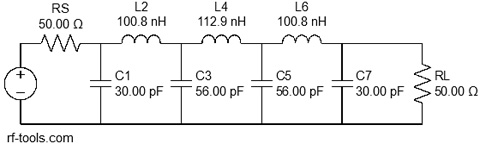
When assessing filter performance for an FM transmitter, given that the frequency reponse drops linearly (except for Cauer filters) as frequency increases, the worst performance will be at harmonics of 87.5 MHz. Whatever is achieved at that frequency will be bettered at harmonics of 108 MHz which is higher in frequency. The filter illustrated above has a largely flat frequency response to around 113 MHz, and then attenuates harmonics as follows.
| Harmonic | Frequencies | Attenuation |
|---|---|---|
| 2nd | 175 MHz 216 MHz | 36 dB 51 dB |
| 3rd | 262.5 MHz 324 MHz | 64 dB 78 dB |
| 4th | 350 MHz 432 MHz | Better than 80 dB |
Note that these ideal, calculated values will be limited by the method of construction. A filter built on printed circuit board (PCB) in limited space will never perform as well as one constructed in a seperate metal can with each inductor isolated from its neighbours. In practice, a compact, PCB based low-pass filter would struggle to achieve much more than around 60 to 70 dB harmonic rejection but for low power transmitters, this should be sufficient (and indeed meets the Ofcom code of practice) which for a 1 Watt transmitter requires that harmonics and spurious should be 46 dB below the carrier. Given that the second harmonic of the raw FM transmitter, even at 175 MHz, is already more than 10 dB below the carrier the additional 36 dB of attenuation provided by the filter will meet the Ofcom requirements with no difficulties.
How not to design transmitters and receivers (part 8: divide by N)
Friday 3 September, 2021, 08:46 - Amateur Radio, Broadcasting, Licensed, Pirate/Clandestine, Electronics
Posted by Administrator
The next functional block that is required to complete a transmitter (not a receiver for which there are many other blocks to consider) is the 'divide by N' device. In principle, all that is required to achieve this function is a counter which will count up (or down) until it reaches a particular number (or zero), indicate this (i.e. with some kind of output pulse) and reset itself. Posted by Administrator
There are many ways of achieving this from the use of logic ICs to dedicated counter ICs. Let's begin with the logic IC approach. Any binary counter which has a way of being reset to zero can be used as a counter. It's simply a matter of detecting when the right combination of bits have reached '1' and then resetting the counter and starting again. A simple way of doing this is using a CMOS 4020, 4024, 4040 or 4060 counter. To check when a selected number of bits are all 1's, connect the cathode of a number of diodes to the relevant bits, connect the anodes together to a common point and then join that point to positive via a suitable resistor. When any of the bits are zeros, they will pull the common point down to ground through the diodes. Only when all of the bits are 1's will the common point go high. An example circuit, including a switch to decide which diodes (and thus which bits) are tied to the common point is shown to the right (click for a larger version).
;) Pin 11 of the 74HC4020 counter is connected to the positive supply by the 2.2K resistor, and will reset the counter to zero when it goes high. However, this is the common point for the diodes which will pull this point down to ground when any of the bits of the counter switched into circuit are zero. Only when all the bits which are switched into circuit go high will pin 11 go high, at which point the counter resets and will start counting again at the next input clock pulse. The output of the circuit could be taken from the common point, however the reset pulse is very narrow and may be missed by, for example, a slower operating phase comparator. In this example, the output is taken from the second most significant bit, which will give something nearer to a square wave. Note that the diodes have been arranged so that the switches are in binary significance order with the most significant bit being on the right hand side and the least on the left.
Pin 11 of the 74HC4020 counter is connected to the positive supply by the 2.2K resistor, and will reset the counter to zero when it goes high. However, this is the common point for the diodes which will pull this point down to ground when any of the bits of the counter switched into circuit are zero. Only when all the bits which are switched into circuit go high will pin 11 go high, at which point the counter resets and will start counting again at the next input clock pulse. The output of the circuit could be taken from the common point, however the reset pulse is very narrow and may be missed by, for example, a slower operating phase comparator. In this example, the output is taken from the second most significant bit, which will give something nearer to a square wave. Note that the diodes have been arranged so that the switches are in binary significance order with the most significant bit being on the right hand side and the least on the left.This circuit works very well, however it has one minor flaw and one major, yet surmountable one. The minor flaw is that a finite amount of time is required between the common point going high and the counter being reset. This time is measured in nanoseconds, however if the counter is running particularly quickly (i.e. at frequencies measured in MHz where each bit is less than a microsecond long) this delay means that the counter counts to 'N and a bit', the 'bit' being the extra time taken for the counter to reset. Some circuits set the counter to 1 less than is required, and use an additional flip-flop to count the last bit whilst giving the counter time to reset, but this adds extra complexity (and thus cost) to what is an otherwise simple circuit.
The major yet surmountable flaw is that each output pin of the divider has a square wave on it. These pins generate small but nevertheless detectable harmonics right across the radio spectrum. If a prescaler is noisy, these things are deafening and as receivers are very sensitive, these outputs will produce interfering signals at almost any and every frequency to which you may wish to tune unless extreme care is taken to shield this part of the circuit from the receiver parts. Thus, whilst such a design is great in a transmitter (assuming a buffer and/or prescaler is used between the VCO and it), it is a veritable pain in the back-side in a receiver.
There are, thankfully, a number of pre-settable counters which overcome both of these problems. An old device but one which is very easy to use and understand is the TC9122P.
;)
The TC9122P can count from 1 to 3999 and its inputs are in binary blocks of 10 (otherwise known as binary coded decimal, BCD). So to divide by 896 or 1079, the required setting would look something like:
| 0 | 8 | 9 | 6 | 1 | 0 | 7 | 9 | |
| 00 | 1000 | 1001 | 0110 | 01 | 0000 | 0111 | 1001 |
;) Rotary BCD switches are available which could be directly connected to the inputs and then frequencies could simply be 'dialled' in. The same result can also be achieved with a 4059 which is a little more complicated as it has a number of different counting modes including, though, BCD. An example of using BCD switches to dial up a frequency is illustrated on the left (which is taken from a Broadcast Warehouse 1 Watt FM exciter).
Rotary BCD switches are available which could be directly connected to the inputs and then frequencies could simply be 'dialled' in. The same result can also be achieved with a 4059 which is a little more complicated as it has a number of different counting modes including, though, BCD. An example of using BCD switches to dial up a frequency is illustrated on the left (which is taken from a Broadcast Warehouse 1 Watt FM exciter).In part 7 of the 'How not to design transmitters and receivers' the MC145151 was introduced. This IC includes a divide by N counter which is a straightforward binary (and not BCD) counter. One oddity with that particular chip is that the input pins to the counter are tied high with an internal resistor meaning that pins which need to be set to zero should be connected to ground, whereas with many other counters it is usually the pins which need to be set to one which should be connected to positive.
An example of using standard binary to set the numbers 896 and 1079 are shown in the table below.
| Decimal | Binary |
|---|---|
| 896 | 01110000000 |
| 1079 | 10000110111 |
One thing that was noticed when considering using straight binary (and not BCD) for programming frequencies across the FM band is that to select numbers over 1023 (e.g. if using a reference frequency of 100 kHz and wishing to access the whole FM band such that numbers up to 1079 are required), 11 binary digits are required (that's eleven, not three). Nice, cheap, binary switches are available in 10 or 12 bit versions. Whilst it would have been easy enough to use a 12 bit switch and leave one bit unused, it would be even nicer to find a way to use a 10 bit switch.
 Such a way was found. If we call the most significant bit 'bit 11' then bits 9 and 10 can be tied together (as has actually been done in the counter circuit above). This means that any binary number from '01100000000' representing 768, to '10011111111' representing 1279 can be set. Assuming a 100 kHz reference frequency, anything from 76.8 to 127.9 MHz can be set using just a 10 bit switch. In addition (though potentially rather uselessly in this application) any other binary number in which bits 9 and 10 are the same can also be selected. Thus numbers from '00000000000' (0) to '00011111111' (255) and '11100000000' (1792) to '11111111111' (2047) could also be set, potentially representing frequencies from 0 to 25.5 and 179.2 to 204.7 MHz.
We now have nearly all the blocks necessary to create a variable frequency phase lock loop based FM transmitter. There's still the reference oscillator (which is relatively trivial) and low pass filtering to go.
How not to design transmitters and receivers (part 7: phase comparators)
Wednesday 1 September, 2021, 08:31 - Amateur Radio, Broadcasting, Licensed, Pirate/Clandestine, Electronics
Posted by Administrator
One of the blocks yet to be discussed in the Wireless Waffle lockdown transmitter and receiver project is the phase/frequency comparator. In days of yore (a.k.a. the 1980s), the go-to integrated circuit (IC) for this function was the trusty 4046. This not only contains a couple of different types of phase comparator (the newest versions have three, the older ones just two) it also has a built in voltage controlled oscillator (VCO). The VCO works well up to a few MHz, or even higher depending on the specific type of IC, but is useless at VHF and thankfully can be easily inhibited. As, however, the phase comparator only needs to work at the reference frequency (usually a few kHz), the 4046 will function perfectly well in this role.Posted by Administrator
The 4046 takes the reference input on pin 14 (oddly termed the 'signal in' pin) and the variable frequency input on pin 3 (the 'comparator in'). The two phase comparator outputs are on pins 2 ('comparator I output') and 13 ('comparator II output'). On newer versions a third phase comparator output can be found on pin 15; on the older versions pin 15 has a Zener diode connected to it which is intended to be used to stabilise the power supply when using the VCO but was almost never employed.
;)
The Type I phase comparator is just an XOR gate. This produces a square wave output whose mark-space ratio varies with the difference in phase of the inputs. This can be fed into a loop filter to yield a voltage which varies up or down with the difference in phase. The primary difficulty with this method is that both the reference frequency, and the variable frequency input must be square waves with equal mark-space ratios. For the reference which is usually a square wave divided down from some crystal oscillator, this is usually not a problem, however the signal from the oscillator, following its traversal through the 'divide by N' circuit, is often just a pulse. Many divide by N devices just count a specific number of times, and when that count has been reached output a brief pulse. Additional circuitry is required to turn this into a square wave.
The Type II phase comparator is an altogether more sophisticated device and as well as not caring about the mark-space ratio of the two input signals, produces a positive 'up' or negative 'down' signal at its output instead of just a square wave. If its output is connected to a capacitor (through a suitable current limiting resistor) the voltage across the capacitor will only be given a push up or down if the phase of the input signals is different. If the two are fully in phase, the output of the Type II detector is an open circuit. This massively reduces the amount of the reference frequency that appears at the input to the loop filter, making the whole PLL output cleaner. When modulating the VCO, there will almost inevitably be occasional phase differences so the output will rarely be totally quiet, but this type of detector is generally far easier to work with.
Most modern PLL ICs have a reference oscillator and divider, the divide by N counter, and the phase comparator functions included in them in a single package. Some even have built-in prescalers. Even some older devices integrate several of these functions. The MC145151 which was commonly used in many of the CB radios of the 1980s contains all except the prescaler. The phase detector in this device is akin to the Type II device in the 4046 but has two separate outputs:
- a single pin output mimics the operation of the 4046, with positive and negative pulses and an open circuit when the reference and VCO are in phase, and
- seperate 'up' and 'down' pins which need to be fed into an external combiner/loop filter to generate the voltage to feed the VCO.
;)
How, then, to get a bigger voltage swing? One method would be to feed the output from the phase comparator into an op-amp with a higher supply voltage, and set up with a gain profile which steps up the 5, 9, 12 or whatever voltage is available from the phase comparator to a higher value. The circuit pictured above will do this. The input from the phase comparator first goes through the previously discussed 'lead-lag' low pass filter. The op-amp is set to have a gain of 2.4, so that a 5 Volt input will give a 12 Volt output. This amplifier, as well as increasing the voltage swing will also, however, amplify any noise at the output of the phase comparator and thus is not ideal.
This is where the seperate 'up' and 'down' pin output of devices such as the MC145151 come into their own. Given that there has got to be an external loop filter to use these outputs, this could by default run from a higher supply voltage. Also, as the signals are only nudges up or down, the active loop filter that follows would not further amplify any noise generated by the phase comparator.
;)
The circuit above gives an example of this and has a similar frequency response to the earlier amplifier circuit. It has has a differential input: A positive nudge on the 'V up' input will cause the output voltage to rise and similarly a positive nudge on the 'V down' input will cause the output voltage to fall. When both are silent, the output voltage will hold steady. In this steady state, no noise is being generated or amplified making this kind of approach relatively quiet.
Of course in most cases a 30 Volt supply won't be available (though one could be generated using a simple charge pump but that's for another day), however supplying the amplifier and thus the VCO from even a 12 Volt supply will give an improved frequency range compared to 5 or 9 Volts.